MODULE 7 PLASMA DISPLAYS 71 INTRODUCTION THE REALIZATION OF
BINDING IN ALEPH OPEN THE ACQUISITIONSSERIALS MODULEMODULE 1 INTRODUCTION À LA FORMATION
MODULE 12 AIRES PROTEGEES TRANSFRONTALIERES
MODULE 3 DEFINITIONS CHAMP D’APPLICATION PRINCIPES
MODULE 6 REGLEMENT ÉVALUATION DE L’IMPACT
MODULE SPECIFICATION IMPORTANT NOTES – PLEASE READ
Plasma Display Panel
Module 7: Plasma Displays
7.1. Introduction
The realization of having a large 60 inch diagonal flat panel display hanging on your living room wall is here in the form of a [plasma display. Color plasma displays utilize the physical phenomena of gas discharge and are sometimes referred to as glass discharge displays - the same physical principle as fluorescent lamps. A gas discharge generates ultraviolet light which excites a phosphor layer that fluoresces visible light. Plasma displays are often classified as ac or dc which describes the method of current lighting. The pioneering working gas discharge closely parallels the early discoveries in electricity because its impressive luminous output that enticed the early researchers to study electricity. Jean Picard is generally accredited with the first gas discharge demonstration in 1678. However, continuous gas discharge had to await the development of the battery by Volta in 1800. In 1838, Faraday performed the first experiments of gas discharge between two metal electrodes placed in an evacuated glass bulk, much like display configurations. Since the early discoveries of plasma discharge, the technology bias progressed to its current 60 inch diagonal full-color configuration.
7.2. Positive Attributes of Plasma Displays
The electrical characteristics of gas discharge (i.e. non-linearity and memory) allow plasma display panels to be made very large (i.e. in the 20 - 60 inch diagonal range).
Good gray scale capability. All digital gray scale allows at least 256 levels of gray.
Plasma posses a very large non-linearity (i.e. strong threshold). For applied voltage below threshold (i.e. firing voltage) the display emits practically no light; therefore, a large number of lines can be addressed enabling high resolution. 1280 x 1024 has been demonstrated. The high level of non-linearity is a considerable advantage when compared to liquid crystal displays. A liquid crystal material is not very nonlinear, and therefore some other nonlinear element must be implemented on the substrate such as a thin film transistor to increase display non-linearity.
Plasma displays possess inherent memory. Memory is a highly desirable feature since a large number of rows (high resolution) can be addressed. This is because a display with memory has a pixel duty cycle of one. Displays without a memory function have a pixel duty cycle of one divided by the number of scanned lines. For non-memory based displays get bigger and the number of scanned lines increases, the duty cycle and therefore, the brightness of the display decreases. Also, memory removes any flicker sensation.
Plasma display panels have a long lifetime, comparable to CRT displays. Then half luminance lifetimes have been reported to range between 10,000 to 30,000 hours.
Plasma displays have a very wide viewing angle since their emission is Lambertian.
Full video is possible since plasma can switch on the order of microseconds.
The luminous efficiency is good (450 cd/m2 at 1 L/W).
Color plasma displays have many common equipment needs as CRTs for manufacturing, which is substantially less than a semiconductor manufacturing line needed for active matrix LCDs.
Plasma display panels are mechanically robust because of their rugged self-supporting structure. They are known to be high shock and vibration tolerant and have therefore been heavily utilized in military applications.
Plasma displays have a characteristically high impedance which makes them easy to drive. The driving electrode capacitance is very low because the dielectric constant of the gas is essentially one. This is the lowest electrode capacitance of any display on the order of 103 times smaller than electroluminescent and 102 times smaller than liquid crystal displays. This translates into current requirements and smaller drive circuit silicon for plasma displays. They are high voltage devices (~100V), the current is very low - high voltage drives are easier to design than high current drivers. Large area panels can be designed with little power dissipation.
Plasma displays can be designed 100% digital - important for new future applications such as digital video disks and high definition television.
The color gamut of full color plasma displays is adequate - slightly smaller than that of a CRT.
Plasma displays do not scatter ambient light like their CRT counterparts.
7.3. Electro-optic Performance of Plasma Displays
The basic operation principles of gas discharge or plasma will be discussed here, followed by a more elementary treatment of the underlying physics and physical chemistry of gas discharge.
7.3.1. Current - Voltage Characteristics
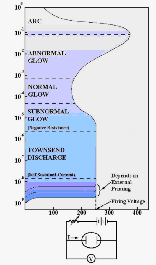
One of the most advantageous electrical properties of plasma in the context of a display application is its strong non-linearity at the firing voltage which enables matrix multiplexing addressing. The current-voltage (I-V) curve of a conventional plasma display is shown in the figure. It is important to emphasize that the I-V curve is presented on a semi-logarithmic scale where the current transcends nine orders of magnitude and the inherent non-linearity is 'built-in' to the material. The figure is subdivided into several regimes, from arc to Townsed discharge and when the discharge current has sufficient magnitude, space charge distortion sets in resulting in a negative resistance region. A typical plasma display would operate near the junction of the normal glow and abnormal glow regions.
Now, let's revisit one of the most attractive features of plasma display - the extreme non-linearity of the the gas discharge phenomena. The figure depicts the firing voltage at approximately 250 V. Note the extreme sensitivity of the current scale in this region; for small small charges in voltage the current can change by as much as three orders of magnitude. The light output of the plasma display is approximately proportional to the current; therefore, plasma is ideal for multiplexing schemes.
The gas discharge process requires external priming as identified in the low current (nA region) region of the graph. The gas discharge process requires some energetic particles begin the avalanche process (discussed next) for at least one electron to initiate the growth discharge process. Without priming, the discharge process will never commence at any voltage. Priming electrons can come from a number of different active particles created by a prior discharge or even by a neighboring discharging pixel. The active particles can include many different species - free electrons, free ions, metastable atoms and ultraviolet photons.
The I-V characteristics of a plasma gas discharge display show that current levels can reach very large values, and to avoid a catastrophic arc, some current limiting mechanisms must be introduced. The figure below illustrates two ways of accomplishing this which have been utilized successfully in commercial displays.
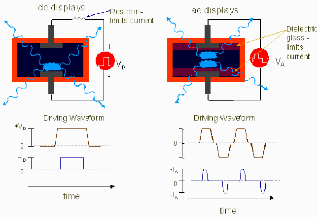
Plasma displays based on dc use a resistor, a semiconductor current source, or a short voltage pulse to limit current and have the electrode in intimate contact with the gas. For the ac mode, on the other hand, the current is limited with an internal glass dielectric that couples the electrode's capacity to the gas discharge.
For systems used commercially, dc displays have the resistors or current sources connected to the display electrode external to the panel which allows one discharge to be ignited along that electrode at any one time. For scanned displays, this approach works fine. Multiple discharges and dc memory require placing the resistor internal to the panel in series with each pixel, or a resistor per sub-pixel.
The ac displays achieve memory and current limiting with a dielectric layer. The dielectric layer acts as a capacitor in series with each pixel. The discharge deposits a charge on the wall that reduces the voltages across the gap when a voltage pulse is applied to an ac panel. After a short time period, the discharge will extinguish and the light output will end until the applied voltage reverses polarity and a new discharge pulse occurs. This results in an inherent memory function which greatly increases the size of the display while maintaining brightness.
7.3.2. Wavelength Output Distribution
For display applications, the optical output in the visible region is of most importance. The figure below shows the wavelength distribution.
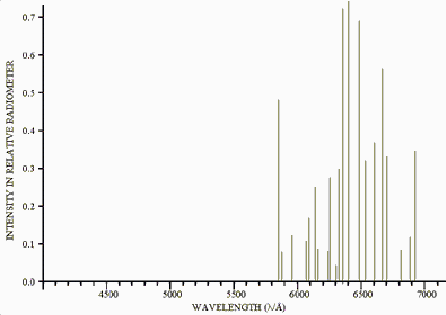
This is a typical spectrum of gas discharge phenomena of neon gas. The major reason for using neon in plasma displays is its high luminous efficiency among the noble gases. The above spectrum gives a common neon orange color emitted by most plasma displays. Other colors are achieved by using other gases or by introducing phosphors into the display.
7.3.3. Regions of the I-V Curve
There are several regimes of the I-V curve that need to be treated. These are the following:
Low current regime
Townsed discharge regime
Subnormal glow regime
Normal glow regime
Abnormal glow regime
Arc regime
Low Current Regime: The lowest currents are in the 10-8 - 10-9 regime that are strongly dictated by the priming process. These low currents are below the firing process.
Townsed Discharge Regime: As firing voltage is exceeded, current grows rapidly, as discussed earlier. In this regime, current is constant in a very wide range. This regime is often referred to as the self sustaining regime because the gas discharge phenomenon will continue after priming current is removed.
Subnormal Glow Regime: These can eventually result in a negative resistance region because the density of charged particle in the gas will reach a point where it influences the applied electric field.
Normal Glow Regime: Once, the space charge distribution is established, the discharge will configure itself such that the current density on the cathode surface is constant. The variation in current in the normal glow region occurs by varying the area of the negative glow that fills the cathode so constant density is maintained.
Abnormal Glow Regime: At some point upon increasing the current, the cathode is fully covered with negative glow - constant current density can no longer be sustained. The increase in current density requires a less efficient electric field profile that requires higher voltage across gas. Therefore this region has a positive resistance.
Arc Regime: At high currents, the power dissipation in the discharge is so large and temperature is so enormous, that the cathode material is vaporized. The cathode vapor creates a very high pressure gas that can support the high currents which generates a high degree of field distribution. At this point, since the temperature and fields are so high, both the atomic and field emissions are the dominant cathode emission mechanism. High currents can be generated in this regime for voltages of <10 Volts. The arc is therefore characterized by a sharp negative resistance curve. These large currents will result in catastrophic failure of a display, so the significance of understanding the arc phenomenon is not to let it happen.
Within the normal glow discharge regime there are three regions commonly observed:
Negative glow
Faraday dark space
Positive column
Negative Glow Region: There is a high E field region near the cathode where most of the voltage drop occurs. In this region, strong avalanches develop which generate light output associated with the negative glow.
Faraday Dark Space: After the field is near the cathode is terminated, the electron current is still high. However electrons do not have very much energy because E is low and thus light - therefore light generated is low resulting in a dark space.
Positive Column: The next region toward the anode is the positive column. and electrons are contained in this region. In this region, electron and ion density are comparable, the E- field in this region is of low constant value, and mobility of ions and electrons is unimportant since field is low.
7.4. The Underlying Physics of Gas Discharge
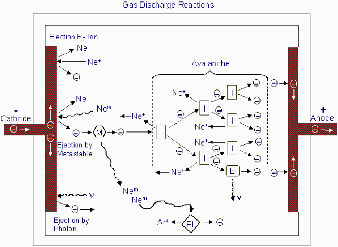
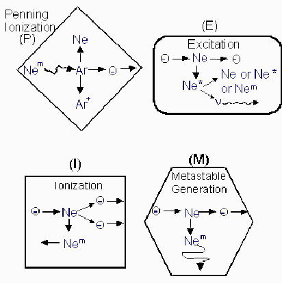
Here we will review the underlying physics of gas discharge in a relatively simple form. There are several reactions that will be covered here. We will work with the example of the Penning Mixture - a neon gas doped with a small percentage of argon (< 0.1% Ar).
We will categorize the reactions as gas volume reactions and cathode surface reactions. The gas volume reactions are ionizations (labeled I), excitations (E), metastable generations (MG) and Penning Ionization (PI). The cathode surface reactions are concerned with the ejection of electrons from the cathode by ions, metastable atoms or photons.
|
|
Electron |
- Drift Right |
|
Ne |
Neutral Neon Atom |
- Diffuse |
|
Ne+ |
Positive Neon Atom |
- Diffuse |
|
Ar |
Neutral Argon Atom |
- Diffuse |
|
Ar+ |
Positive Argon Atom |
- Drift Left |
|
Ne* |
Excited Neon Atom |
- Diffuse |
|
Nem |
Metastable Neon Atom |
- Diffuse |
|
n |
Photon |
- Propagate |
Even in the simplest explanations, the gas discharge is complex. It has many species that are transported by different mechanisms. The type of species found in this example are the following:
electrons
neutral neon atom
positive neon ion
positive argon ion
excited neon atom
metastable neon atom
photon
The charges species in the gas discharge reaction include electrons, positive neon ions, and positive argon ions and are transported by the electric field i.e. field induced drift. Diffusion transport is considered secondary to the field induced drift mechanism. The neutral species include the neutral neon atoms, the neutral argon atoms, the excited neon atom, and the metastable neon atom. Because of their neutrality, their transport is governed by diffusion. Photons are governed by the laws of electromagnetic radiation.
7.5. Gas Discharge Reactions
7.5.1.
Energy Level Diagram for Neon
The figure below shows the allowed transition for an outer electron of the neon atom.
|
|
optical
output due to |
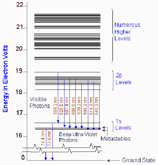
The optical output of the gas discharge process is strongly correlated to the above energy level diagram. The optical output spectrum shown above is a consequence of photon emitted when an excited neon atom makes a transition between the 2p and 1s energy levels.
Ionization is the most vital reaction of a gas discharge used in plasma displays. When an electric field is applied across the gas, the electrons within the gas are accelerated and collide with neutral gas atoms. The figure above demonstrates that the new atom has NO allowable energy levels between 0 and 16.6 eVj; therefore most collisions will be elastic in nature. Elastic collisions means that election does not gain or lose energy. As shown in the above figure, 21.6 eV is the ionization limit of the neon atom and the electric field will undoubtedly have accelerated elections to this level.
These collisions can cause an electron to be ejected from the neon atom theory creating a positive neon ion and a new free electron.
The ionization reaction is given by:
Ne + e- --> Ne+ + 2e-
Both the ion (+) and electron (-) drift in the field in opposite directions. Since the neon ion is massive compared to the electron, it drifts 102 times slower.
Excitation will occur. Some of the electrons will gain sufficient energy to excite the neutral neon atom during a collision. This reaction occurs between 16.6 - 21.6 eV. For energies less than this only elastic collisions result and above this, ionization is favored.
The time scale of the excited atom is 10 ns, which is short, before it radiates a photon and returns to the ground state. The reaction is described by:
Ne + e- --> Ne* + e-
Ne*--> Ne (or Ne*, or Nem) +v
The spectrum observed for a plasma display panel are layers, a result of the transitions between 2p and 1s levels. This leaves the atom in the excited 1s state that will undoubtedly be deexcited by some later reaction.
There are a number of metastable levels in the energy level diagram that is shown above. There are two of four 1s levels of neon that cannot emit a photon, i.e. metastable. The reaction can be written as:
Ne + e- --> Nem + e-
These so called metastable states can also be created as a by-product by an excitation reaction. Many of the radiating transitions shown in the energy level diagram end up in one of the two metastable levels. A two step process can therefore cause metastable generation - e.g. > 18.5 eV excites a neutral neon atom to the 2p state and that atom radiates a photon, forcing the neon atom in the 1s metastable state. This two step process is:
Ne + e- --> Ne* + e-
Ne*--> Nem + v
The transport diffusion process of metastable atoms is slow since the neon atoms do not radiate a photon and are therefore neutral. Positive neon ions are virtually the same mass, but move much faster since they are charged. Metastable atoms survive for long times - on the order of 1-10 µs - significantly longer than the 10 ns lifetime of excited atoms. Metastable states do not naturally decay but are typically dexcited by collisions with the chamber walls or the Penning ionization process.
Metastable atoms have ~16.6 eV of energy in the energy level diagram. This additional ionization phenomenon enables plasma display panels to switch at lower voltages. The argon atom concentration strongly dictates the additional ionization. Penning described the concentration, about 0.1% in Neon, to provide the largest amount of ionization per applied volt. This is known as the Penning mixture. Other Penning mixtures include neon, xenon, krypton, and noninert gases.
There are a number of important reactions at the cathode surface. Electrons can be ejected from the cathode surface, which can be simulated by cathode collision from positive ions, metastable ions, and photon. The most important cathode surface reaction for plasma displays is the electron ejection due to positive ions. The energy of neon and argon is:
|
Energy |
|
|
Argon Ion |
15.8 eV |
|
Neon Ion |
21.6 eV |
Upon collision with the cathode, the ions capture an electron from the surface and become neutral - thereby saving up their energy to the surface. The energy is sufficient to allow the electron to escape the work function energy of the cathode surface, which is in the range 3-10 eV. The significant portion of electron energy results in a high probability that an ion colliding with the surface will result in electron ejection. The ejection reaction is dominant in plasma displays because all ions in field are transported in the field, and additionally drift toward the cathode.
The photo emission phenomenon is also an important mechanism for electron ejection. Because of the nature of the work function of the cathode, ~3 eV, only ultraviolet photons have significant photoemission. These ultraviolet photons have transitions between the 1s and ground state energy levels. These ultraviolet photons are emitted isotropically and even though there are a lot of them, only a few are directed toward cathode.
Metastable neon atoms have an energy of 18.8 eV that can be given to the surface to eject an electron and dexcite the metastable atoms. The metastable atoms are not as nearly important as the ions since they tend to diffuse in random directions at very slow rates as compared to the transport of ions towards the cathode.
There is also a phenomenon in plasma display called an Avalanche. Because the ionization reaction discussed above results in two free electron and a positive ion, an avalanche can occur. The two electrons can then go on to create two more ionizations, and continue to do this over and over again. As the avalanche grows and progresses to the anode, the number of ionizations increases exponentially. For plasma displays, 10-300 ionizations can occur in an avalanche.
7.5.2. Modeling Gas Discharge
Simple models are useful in understanding plasma display phenomenon - firing voltage, current growth rate, and priming.
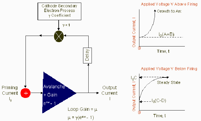
The avalanche process can be modeled as a simple amplifier with gain circuit shown above. The gain is given by
Gain µ = e v - 1
Where is the number of ion pairs per volt and V is the voltage across the anode and cathode.
The magnitude of strongly depends on the gas mixture, gas pressure P, and the electric field E. The for neon doped with 1% argon is much larger than for pure neon because of the Penning reaction.
Avalanches create ions, metastables, and photons which can find their way back to the cathode and eject secondary electrons. The avalanche gain increases with increasing voltage. Since secondary electrons can now start new avalanches, these process can be modeled as a feedback path in the circuit. The delay depicts transient time for the ions, metastables, or photons between point of creation and cathode. There is a finite probability, that the particle will cause an ejection of an electron when it reaches the cathode. The term is a multiplicative to the feedback term.
The secondary electrons that are ejected from the cathode must be added to the electrons due to the priming current I0. The priming current comes about from external means such as photoemission from photons (generated by an independent nearby gas discharge). The sum of the priming and secondary current represents the flow of electrons that can start new avalanches, and can feedback into gain amplifier - i.e. positive feedback.
The loop gain model is easy to understand. If the loop gain is greater than 1, it will become unstable. The loop gain is defined as
µ = (e v - 1)
where µ = 1 is a point of instability. This condition defines the firing voltage of the gas discharge.
The transient behavior of the current depends output current for V above firing is shown in (b). the current grows exponentially with a positive time constant , which is correlated to µ and the feedback delay time:

where
A and B are constants, and I0
is the priming current. The output current I is proportional to the
priming current I0.
Once initiated, the output current will experience growth until some
other phenomenon limits it. Catastrophic failure results if the
current continues to grow until an arc appears - therefore some
current limiting mechanism must take over.
The current growth for V below firing is also shown in the figure. In this situation <1, so the output current asymptotically approaches a steady state value.

As with the situation above firing, the coefficients C and D are independent of time, and I I0.
Since I I0, the gas discharge phenomenon will not occur without some external priming current. Priming can be as simple as a single electron to initiate the avalanche. Without a single electron, the gas discharge process cannot occur, no matter how much voltage is applied. The three priming procedures are pilot cell priming; self-priming; and radioactive priming.
Pilot cell priming is the most common on plasma display technology. The pilot cell will generate electrons, ions, photons, and metastables derived from the discharge. The various reactions occurring in gas discharges, thus will create electrons in the cell to be initiated.
The importance of these particles is the priming process largely depends on the space (distance) between the pilot cell and prime cell. The electron and ions will usually follow the electric filed lines and will therefore be influenced if the primed cell and pilot cell are close. The metastable ions are only important in the priming process when the prime and pilot cell are in close proximity. The metastables contribute to priming by the Penning effect or by colliding with the cathode and ejecting an electron by the cathode secondary process.
A sufficient number of photons will also be created in the pilot cell, which can in turn create electrons in the primed cell by photo-emission. Typically, photoemission only occurs for deep ultraviolet photon. This is typically not an effective prime because the ultraviolet is strongly attenuated through the glass. If the photons are unobstructed, most photons will travel freely without much absorption by gas. For this case, photons have a large range priming influence, and distance between the pilot cell and prime cell can be large.
Self priming is another option in the case when the pilot cell and primed cell are the same. This is utilized when the cell is periodically pulsed. If the period since the last discharge pulse is relatively short, there still may be priming particles left around (electrons, ions, metastables, and photons). These can be utilized in the next discharge. However, for self priming, the display needs some priming mechanisms when it is first turned on. Care must therefore be taken to ensure that the critical starting particle decay time between discharges is not exceeded by normal operation, otherwise cell will not execute a discharge.
A type of priming rarely used is radioactive where small amounts of radioactive gas is doped into the gas mixture (Kr 85, Ni 63). The radioactive particles emitted will have sufficient energy to ionize a large number of atoms. This is an attractive solution to priming because no additional prime cell is needed but radioactive particles do present a health risk during manufacture. Once enclosed in the glass envelope, beta particles do not penetrate the glass for the Kr 85 and Ni 63 elements.
One of the most important issues to plasma display engineering is the dependence of firing voltage on the gas discharge cell design. This is characterized by the Paschen curve shown below.

The curve provides the breakdown voltage as a function of pd, the gas pressure and the separation between the cathode and anode. It is important to note that the firing voltage will remain unchanged for differing cathode - anode distances as long as the pressure is changed so that the product pd is a constant. This is commonly utilized by display engineers to minimize cost. In order to reduce drive circuit costs, it is desirable to have a low firing voltages. The value of d is usually dictated by resolution so the display engineer has the freedom to choose p for a given d to minimize the firing voltage.
7.3.3. Regions of the I-V Curve
There are several regimes of the I-V curve that need to be treated. These are the following:
Low current regime
Townsed discharge regime
Subnormal glow regime
Normal glow regime
Abnormal glow regime
Arc regime
Low Current Regime: The lowest currents are in the 10-8 - 10-9 regime that are strongly dictated by the priming process. These low currents are below the firing process.
Townsed Discharge Regime: As firing voltage is exceeded, current grows rapidly, as discussed earlier. In this regime, current is constant in a very wide range. This regime is often referred to as the self sustaining regime because the gas discharge phenomenon will continue after priming current is removed.
Subnormal Glow Regime: These can eventually result in a negative resistance region because the density of charged particle in the gas will reach a point where it influences the applied electric field.
Normal Glow Regime: Once, the space charge distribution is established, the discharge will configure itself such that the current density on the cathode surface is constant. The variation in current in the normal glow region occurs by varying the area of the negative glow that fills the cathode so constant density is maintained.
Abnormal Glow Regime: At some point upon increasing the current, the cathode is fully covered with negative glow - constant current density can no longer be sustained. The increase in current density requires a less efficient electric field profile that requires higher voltage across gas. Therefore this region has a positive resistance.
Arc Regime: At high currents, the power dissipation in the discharge is so large and temperature is so enormous, that the cathode material is vaporized. The cathode vapor creates a very high pressure gas that can support the high currents which generates a high degree of field distribution. At this point, since the temperature and fields are so high, both the atomic and field emissions are the dominant cathode emission mechanism. High currents can be generated in this regime for voltages of <10 Volts. The arc is therefore characterized by a sharp negative resistance curve. These large currents will result in catastrophic failure of a display, so the significance of understanding the arc phenomenon is not to let it happen.
Within the normal glow discharge regime there are three regions commonly observed:
Negative glow
Faraday dark space
Positive column
Negative Glow Region: There is a high E field region near the cathode where most of the voltage drop occurs. In this region, strong avalanches develop which generate light output associated with the negative glow.
Faraday Dark Space: After the field is near the cathode is terminated, the electron current is still high. However electrons do not have very much energy because E is low and thus light - therefore light generated is low resulting in a dark space.
Positive Column: The next region toward the anode is the positive column. and electrons are contained in this region. In this region, electron and ion density are comparable, the E- field in this region is of low constant value, and mobility of ions and electrons is unimportant since field is low.
7.6. Time Varying Characteristics
Pulse voltages are applied to plasma panels so the transient behavior must be understood. The engineer needs to know the time for the discharge to grow to a steady state value so the duration of the pulse, pulsewidth, can be incorporated to ensure that the discharge will emit light for a given duration. The after glow, or delay of gas discharge, is important because it determines the subsequent initial densities of priming particles for subsequent discharge pulses. The afterglow characteristics influence the repetition rate.
The two important times during initial growth of discharge are statistical decay and formative decay. The decay is the sum of the two, in the range of 100 ns - 100 µs.
Statistical Decay: A decay time scale is required for one electron in the gas volume to initiate the avalanche. This electron is derived from the priming current I0.
Formative Decay: A time associated with waiting for the discharge to reach its desired current level once the growth discharge has emerged,
Afterglow Decay: A duration where glow persists after the applied voltage is removed. This visible light decays very rapidly, but many other particles in the discharge decay much more slowly and influence the priming of subsequent discharges.
7.7. Plasma Display Technology Fundamentals
There are two types of plasma panels, ac and dc. In the figure below one can compare and contrast them. The main difference between ac and dc is the dielectric film in the ac mode that serves to limit the discharge current and stores charge to increase memory.
7.7. AC Plasma Displays
Color plasma displays are persuaded and dominated by ac technology, so we will focus on ac here. First, starting with the monochrome plasma display to build up, the fundamentals understanding to be applied to full color.
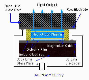
The above ac monochrome structure is produced by depositing thin film electrodes on the front and back glass substrates, and by depositing a thin dielectric layer over the electrodes. The dielectric coatings serve as a capacitator to limit discharge current. The dielectric also stores charge, providing a bistable memory function., The substrates are sealed around the perimeter and filled with neon gas. The simple structure enables pitches to be isolated simply by the action of electric fields.
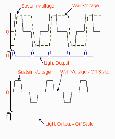
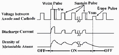
The ac plasma panels require an additional coating of magnesium oxide (MgO), which enables lower drive voltages and extends the life of the panel. The ac displays require an ac signal, often called the sustaining voltage, to be applied during operation. The frequency of the applied voltage is usually 50 KHz. The figure below shows a driving waveform for a pixel in both the on and off states. When a pixel is discharging, charge accumulates on the dielectric glass walls and therefore influences the voltages across the gas. the component of voltage due to this change is simply known as the wall voltages. In the on state, the voltages change for each polarity reversal of the sustained voltage. The change in wall voltage coincides with a pulse of light due to the gas discharge. When the pixel is off, there are no light pulses, and the wall voltage remains at zero level. Pixel addressing is achieved through a partial discharge by introducing an addressing pulse that has time between sustain pulses. A write pulse causes the wall voltage to transmit from zero to the final wall voltage level. An erase pulse causes the wall voltage to return to zero.
7.8. Color Plasma
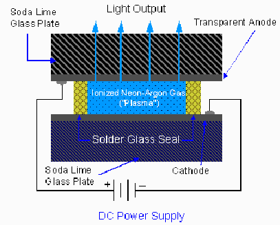
Full color plasma displays are achieved using phosphor. The phosphors are excited by ultraviolet light resulting from the gas discharge process. This is like a fluorescent light. Xenon, doped with neon and helium buffer gas, generates ultra violet light.

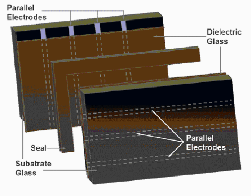
The basic structure of two ac configurations are shown above. The double substrate structure is very simple. The single substrate structure separates the discharge cathode areas from the phosphor by applying the sustained voltage only to the lower electrodes while the phosphor is on top. The single substrate technique results in longer phosphor life because it is not directly sputtered by the energetic ions that are directed toward the cathodes.
The structure for a single ac plasma display is presented above, showing that front and back substrates have a single one dimensional feature. Since the two substrate structures are positioned orthogonally, alignment is not critical between substrates because pixel will automatically arise wherever electrodes intersect, i.e. easy to manufacture.
The phosphors are pumped with the ultraviolet light. In both cases the sustaining electrodes are on the top surface plate. The ac voltage is applied in the conventional way, and the fringing field profile provides the optimal pump.
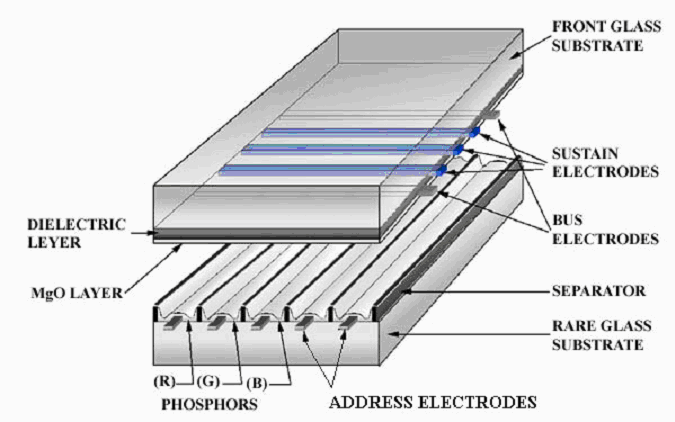
The structure above has glass barrier ribbed spacers between each subpixel, in order to reduce cross-talk between pixels. Reducing cross talk is important in order to retain good color, putting the attenuation of the ultraviolet photons within the ribs does not transmit the 147 nm to 173 nm wavelengths radiated by the xenon gas. The phosphors are placed on the subpixel channel except for the front plate which has the phosphor damaging sputtering activity at the cathode.
Also notice in the above figure that the electrodes are buried beneath the phosphors of the neon substrate. These are the column electrodes that are selectively pulsed depending on the input data. The address activity could potentially cause sputter damage of the phosphor, the address pulse frequency is well above the sustain frequency (orders of magnitude) the amount of address damage is minimal.
The sustain electrodes are made of a conductive transparent material such as tin oxide - however the resistance is orders of magnitude too high. Narrow bus electrodes of high conductivity material, such as silver chrome - copper - chrome, are placed on the tin oxide to reduce electric resistance to values ~100.
The double ac device has a few differences. The main differences are the introduction of glass banner ribs to maintain color purity and the introduction of phosphors. The phosphors are placed on the substrate and are painted to avoid the location directly over the electrode, since the sputtering action and the electrode will cause phosphor degradation.

The figure above shows another color plasma structure. In this configuration there is a placement of resistors in series with each subpixel to limit discharge current for the dc case. Another difference is that the dc device needs to have barrier ribs for all four edges of each subpixel. This is needed to prevent dc discharge for spreading to neighboring pixels. The color arrays are patterned along each row and each column In a two dimensional structure, requiring careful alignment.
Inherent memory can be utilized for the dc plasma structure with the pulse memory waveforms shown below.
The basic principle is a metastable priming from the preceding discharge pulse, then the discharge will build up in a sufficiently short time to fully mature during the very short electrode voltage pulse. The electrode voltage pulse is adjusted to be short to inhibit a sequence of discharges if there has not been an initiating higher amplitude address pulse.
Memory cannot be used to create gray levels since the pixels must be on or off (binary). Instead memory displays achieve gray levels by the percentage of time that the pixel is on in a given frame - therefore pixels must be addressed multiple times per frame.
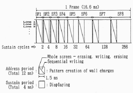
DRIVING SEQUENCE FOR 256 GRAY SCALE
In the figure above for 256 levels of gray, each frame is divided into 8 subfields and each subfield consist of an address period and sustain period. During a given address period, address pulses are applied to all pixels in he panel according to the image date. Each of the eight subfields has a sustain period with a different number of sustain cycles which emits an amount of light proportional to the number of sustain cycles. Each bit of a given pixel intensity is allowed to control one of the subfield, then the total number of sustain cycles (and light) per frame is proportional to 8 bit intensity value. This is digital gray scale.
YEARROUND MODULES [A SINGLE TERM MAY BE
!DOCTYPE HTML HTML LANGEN DIRLTR PREFIXCONTENT HTTPPURLORGRSS10MODULESCONTENT DC HTTPPURLORGDCTERMS
!DOCTYPE HTML HTML LANGES DIRLTR PREFIXCONTENT HTTPPURLORGRSS10MODULESCONTENT DC HTTPPURLORGDCTERMS
Tags: displays 7.1., memory displays, plasma, introduction, displays, module, realization
- 1ª CARRERA DE AUTOS LOCOS DE PELABRAVO NOMBRE DEL
- JERNBANEVERKET SIGNAL KAP 8 HOVEDKONTORET REGLER FOR PROSJEKTERING UTGITT
- ESTATUTOS DEL CONSEJO DIOCESANO DE PASTORAL DE LA DIÓCESIS
- LAS VERDADERAS PÉRDIDAS ISRAELÍES EN LA GUERRA MUNDO
- ces2011-2012_00_00_tra_ac_es1
- 達悟語:索引(以漢語拼音查詢) 以漢語拼音查詢 (CHINESEYAMIENGLISH INDEX) 漢語拼音 中文 達悟語 英文 AI
- POPIS LIJEČNIKA OBITELJSKE MEDICINE MENTORA I INSTRUKTORA NA PREDMETU
- CHAPTER 4 MANUAL MATERIAL HANDLING AND LIFTING TECHNIQUES 41
- PLANTILLA DE EVALUACIÓN DEL ALUMNOA INSTRUMENTOS DE EVALUACIÓN CRITERIOS
- ZĽAVNENÉ JAZYKOVÉ KURZY KTORÉ PONÚKAJÚ JAZYKOVÉ ŠKOLY V TALIANSKU
- LA EVALUACIÓN FORMATIVA 1 LA EVALUACIÓN FORMATIVA ES CONSUSTANCIAL
- M270507 PÁGINA 3 DE 3 HÄFELE NUEVOS SISTEMAS DE
- 01072013 SAYI 2013 1620 ODALARA 38 SAYILI
- THE INFORMATION FOUND ON THIS PAGE IS DERIVED FROM
- MÁS DE 150 PERSONAS DEBATEN SOBRE LA SITUACIÓN DEL
- CATRE COMISIA DE AVIZARE A PRELUNGIRII ACTIVITATII MEDICILOR DUPA
- prestopna_izjava_igralca_2013-2014_ipr
- Mentalni Razvoj o Ovom Broju Revije Želio bi se
- Conducting a Survey 912 i the Purpose
- APELLIDOS Y NOMBRE DNI ASIGNATURA PROFESOR FECHA MEMORIA AUTOEVALUATIVA
- SAVING OUR OCEANSAN URBAN CHALLENGE1 MAYOR JEREMY HARRIS RET
- OCHRONA PRZECIWPOWODZIOWA I JEJ ORGANIZACJA W POLSCE OCHRONA PRZECIWPOWODZIOWA
- PROMULGATION OF AN ANATHEMA AGAINST 2271 BISHOPS OF THE
- DESEO AGRADECER AL SR RECTOR LA OPORTUNIDAD DE PARTICIPAR
- PROTECTIVE MARKING SCHEDULE OF RELEVANT NONSENSITIVE MATERIAL HMA
- FORMULIER TEN BEHOEVE VAN REGISTRATIE VAN ONDERZOEKEN DIE NIET
- SANEAMIENTO DE LOS RÍOS LA CONTAMINACIÓN DE LAS AGUAS
- 10 Kacem Lower Bounds for Tardiness Minimization on a
- T CASOS PRÁCTICOS SERVICIO DE DISPENSACIÓN ALLER SERVICIOS
- ОБАВЕШТЕЊЕ О ЗАКЉУЧЕНОМ УГОВОРУ ЗА ЈАВНУ НАБАВКУ УСЛУГА БРОЈ
81 SVEUČILIŠTE U ZAGREBU FILOZOFSKI FAKULTET UL IVANA LUČIĆA
 PROTOCOLO DE REFERENCIA Y CONTRARREFERENCIA DE GASTROENTEROLOGÍA INFANTIL SSMSO
 SIMBOLOGÍA ELÉCTRICA ÍNDICE 1 NORMA UNEEN 60617 (IEC 60617)
6 OCTOBER 2 2008 EN 323 – VICTORIAN LIT
 WAR OF 1812 3 ALLEN BENJAMIN ALLEN DAVID ALLEN
ROZKŁAD MATERIAŁU Z HISTORII SZTUKI PRZEWIDZIANY DLA KLASY PIERWSZEJ
 INSTITUT RAMON LLULL DIAGONAL 373 08008 BARCELONA
”BOTOX UYGULAMA” İÇİN BİLGİLENDİRME FORMU DR AYCAN KAYIKÇIOĞLU AŞAĞIDA
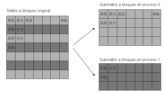 PRACTICAS DE MULTIPROCESADORES PRIMAVERA 2008 PARALELIZACIÓN CON
 DOES INEQUALITY LEAD TO GREATER EFFICIENCY IN THE USE
DOCUMENTS AQMITERRORISME AU SAHELPHILIPPE MIGAUX TERRORISME AU SAHEL
CONTRACT DE ACHIZIŢIE PUBLICĂ DE LUCRĂRI (PROIECTARE SI EXECUŢIE)
 TEMPORADA Nº 64 EXHIBICIÓN Nº 8315 8316 CINEAR CINE
PERATURAN PEMERINTAH REPUBLIK INDONESIA NOMOR 28 TAHUN 2006 TENTANG
LAS LÍNEAS DIRECTRICES 1 OBJETIVOS EL OBJETIVO GENERAL DE
VÁM ÉS PÉNZÜGYŐRSÉG ORSZÁGOS PARANCSNOKSÁGA GAZDASÁGI FŐOSZTÁLY 1122 BUDAPEST
 MEMO MAKING POCKET MONEY IN ENGLISH COUNTRIES IN
VODA – SLOZKA ZIVOTNIHO PROSTREDI HYDROSFERA – VODNI OBAL
TEMPLATE 1A – SPONSOR’S STATUTORY DECLARATION THE SPONSOR SHOULD
 „PŮL NA PŮL“ GENDER STUDIES OPS PUBLIC AFFAIRS
