ARM 64BIT REGISTER FILE INTRODUCTION IN THIS CLASS WE
ARM 64BIT REGISTER FILE INTRODUCTION IN THIS CLASS WE
MIPS 32 by 32 Register File
ARM 64-bit Register File
Introduction:
In this class we will develop and simulate a simple, pipelined ARM microprocessor. Labs #1 & #2 build some basic components of the processor, then labs #3 and #4 create full processors from these pieces.
Building on what you learned from 271, we will use Quartus II and Modelsim for development and testing of your designs. Your processor will mostly be structural (explicit gates and Boolean equations), though the control logic in labs #3 and #4 can be done in RTL (always blocks).
Getting Started:
For many of you, 271 may be a dim memory… but yes, we really did expect you guys to learn that stuff. To refresh your memory, go to the 469 website and go through the 469 Quartus II tutorial. Although we will not be grading anything from that tutorial, these are the building blocks of everything that follows in the lab.
Also on the website is the 271/469 Verilog Tutorial – although I use it for 271, it is set up to contain everything 469 students need to know about Verilog. Go through the tutorial and refresh your memory on each of the elements in there. There are some you might not have used before, such as generate statements, which will come in very handy in this class.
Register File:
For this lab you are to construct a 32 by 64 register file using Verilog. The register file is introduced in chapter 4 of the class text1, with more discussion in Appendix A, section 8. Within the 32 by 64 register file is an array of 32 different 64-bit registers. These registers must be constructed from D flip-flops (positive edge-triggered). Note that for ARM, register 31 is hardwired to always output the value zero, regardless of what may or may not be written to it. The figure below shows a block diagram of a register file.
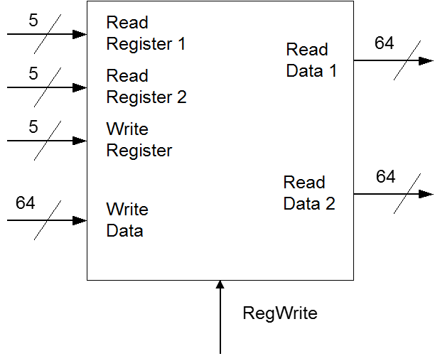
Read Register 1 and Read Register 2 select the registers whose values are output on the Read Data 1 bus and Read Data 2 bus respectively. The Write Register input bus selects the target of the write; when RegWrite is true at the rising edge of the clock, the information on the Write Data bus is written into that register.
Implementation:
A simple implementation of the 32 by 64 ARM register file can be made using registers composed of D flip-flops, a 5:32 enabled decoder, and two large 32x64 to 64 multiplexors. This is shown in the following block diagram (note that the clock is omitted for clarity).
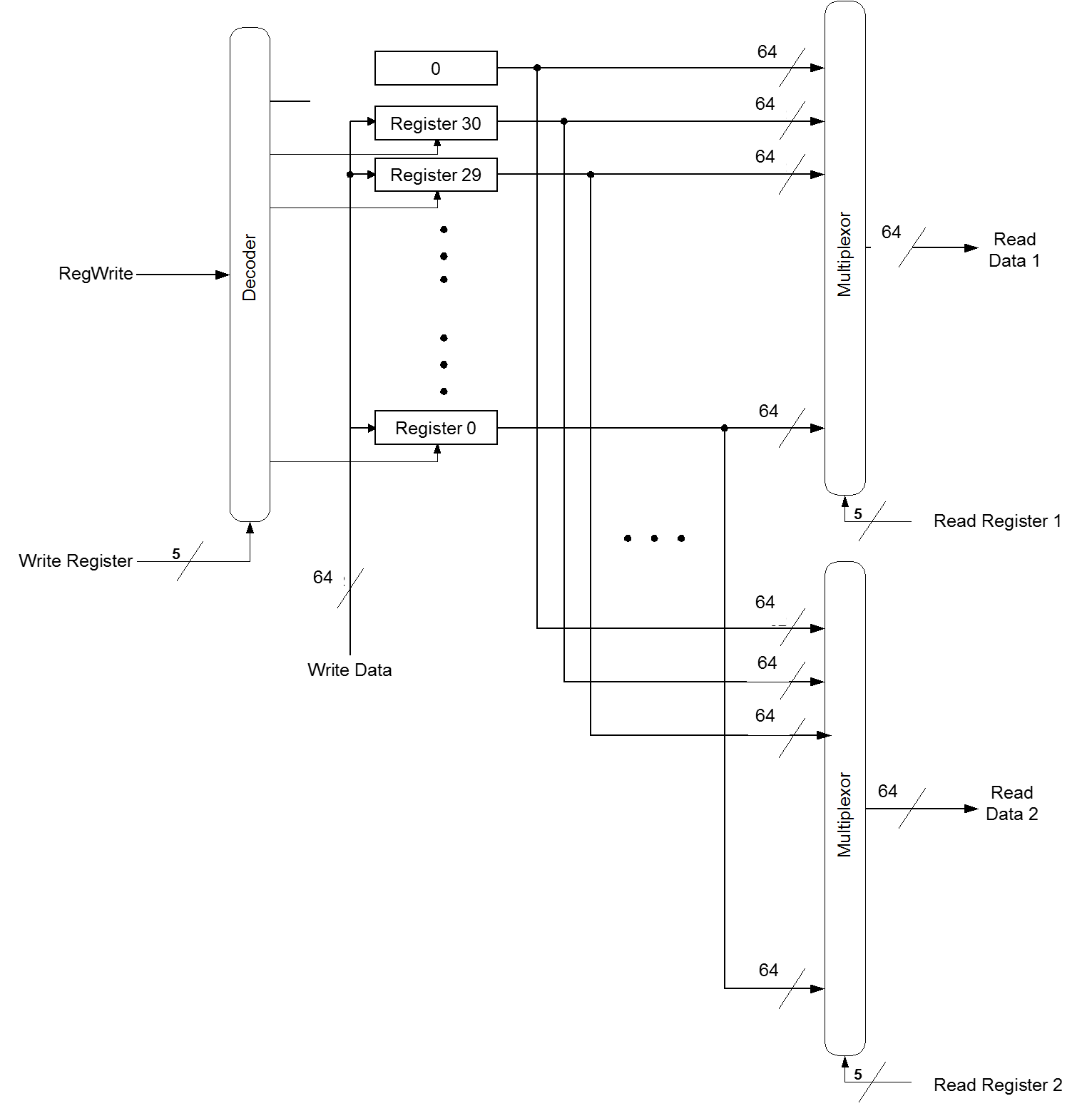
Each register is simply an array of 64 D flip-flops with enables:

Where the D input of each D flip-flop corresponds to a single bit in the 64 bit data input bus and the Q output of each D flip-flop corresponds to the appropriate bit in the 64 bit data output bus. The enable of every D flip-flop is connected to the same write enable input signal. This element will also receive a clock input, which synchronizes the registers. Note that the clock and the write enable are separate signals. The clock is a pure, periodic signal with no glitches or other weird behaviors. The write enable may have glitches and hazards, and thus must be moderated by the clock – make sure that random transitions of the write enable, as long as they are not simultaneous with the activating clock edge (positive edge), do not cause the register to spuriously grab a new value.
The decoder selects which register receives the RegWrite control signal as its enable input. When a register is not selected its enable input should be false. Also note that the most significant output line of the decoder is disconnected in the block diagram for the register file. This is because the 31 register is hardwired to zero so it does not need a write enable input. In fact, instead of using a register, you can just hard-code the inputs to the output muxes for register 31 to all zeroes.
The most difficult part of this lab is constructing the large 64x32:1 multiplexors. One way to do this is to first construct a 32:1 multiplexor and use 64 of these 32:1 multiplexors to construct the larger 64x32:1 mux.
Note that your code for this unit (and in fact all elements of your CPU unless stated otherwise in the lab) CANNOT have any RTL code in it. You can use generate statements (and in fact this is the perfect time to use generate statements..)., You can use “always” blocks for strictly wiring purposes (connecting one signal to another), but no always statements with logic, no always with if statements, etc. All logic in the datapath must be in basic gates, like AND, OR, NAND, NOR, XOR, etc. You cannot even do math operations (+, -, *), nor equality tests (==, !=) – in lab #2 we will build these elements from scratch.
WARNING: On this lab there are easy ways (through hierarchy) and hard ways to do things. If you find yourself writing a LOT of lines that are all identical, except with some bus indexes changed, you are doing it the HARD way – read the section in the tutorial on hierarchy!
Lab Requirements (applies to all labs)
Use the file “regstim.v” as your testbench. You should alter the testing as necessary to make sure your unit works. The TAs will have their own testbench for use during the demos, so you must make sure your register file takes the same inputs & outputs, in the same order, as is presented in the provided testbench.
All logic must be gate level, structural. That is, built from explicit AND, OR, NAND, NOR, XOR, INVERTER, etc. gates. No assign statements (except an assign to set a wire to a constant value or connect wires together), CASE statements, etc. You may use FOR loops to index into buses as needed.
All gates must have at most 4 inputs. You can have procedures with more inputs (and can build larger gates up this way), but the basic gates you will build your circuit out of cannot have more than 4 inputs.
All gates have a delay of 50ps. Processor performance won't be a grading criteria for the class (unless you do really ridiculous things), but you need delay to show how things behave.
You should build all stateholding elements from the D_FF given here.
You may NOT edit it, or change it in any way – if you want
additional functionality, build a module containing one or more of
these D_FF’s plus the appropriate additional logic on the d
and/or q signals. Note: do NOT put any gates on the clk, it will
cause problems! The one exception will be specifically told to you
for lab #4.
module
D_FF (q, d, reset, clk);
output reg q;
input d, reset, clk;
always_ff @(posedge clk)
if (reset)
q <= 0; // On reset, set to 0
else
q <= d; // Otherwise out = d
endmodule
Use this structure to build up all the other stateholding elements and registers in your project.
When we get to labs 3 and 4, you can do the control logic in RTL, or as dataflow (assign statements). The datapath cannot be behavioral at all, except for the DFF, but the control can be built any way you choose.
Your submission should include the files needed to run ModelSim on your design, including a runlab.do file that executes the entire design, and a wave file that sets up the windows properly to illustrates all register contents, output and input ports, clock and reset.
Turn In:
We will use electronic turn-in (check the info on the website) for each lab assignment, and then a demo session to allow you to demo and discuss your lab solution to the TA. Your submission should include all files required to run your project.
** DEMOS ARE REQUIRED, WHETHER YOUR LAB WORKS OR NOT **
If you
do not demo your assignment, you automatically get a 0. Missing your
demo slot without prior approval will impose a late penalty on your
entire lab.
1 “Computer Organization and Design” by Patterson and Hennessy
Tags: 64bit, introduction, register, class
- SOLICITUD DE ADSCRIPCIÓN PARA LA FORMACIÓN EN INVESTIGACIÓN
- IES ABASTOS DPTOGEOGRAFÍAHª HªDEL ARTE PROFESORA CSANFRANCISCO MUSEOS Y
- ETLICHE VON IHNEN WISSEN WIE SKEPTISCH ICH GEGENÜBER EHRUNGEN
- C OMUNE DI VETRALLA PROVINCIA DI VITERBO UFFICIO DI
- D05030502 WYKONANIE WARSTWY ŚCIERALNEJ Z BETONU ASFALTOWEGO DLA KR
- 7 WZORY DOKUMENTÓW STOSOWANYCH W POSTĘPOWANIU PROTESTACYJNYM I ODWOŁAWCZYM
- OVERVIEW CUMPLIMIENTO NOTAS ANEXO TIPOS DE DOCUMENTO
- PERTH AMBOY HIGH SCHOOL 300 EAGLE AVENUE ~ PERTH
- ……… (IMIĘ I NAZWISKO CZŁONKA) (MIEJSCE PRACY) ADRES
- AZ OTP GLOBÁL TREND II TŐKEVÉDETT ZÁRTVÉGŰ SZÁRMAZTATOTT ALAP
- VAKIF KÜLTÜR VARLIKLARI İHALE YÖNETMELİĞİ İHALE SÜRECİNE İLİŞKİN İTİRAZ
- DICE – DIE WÜRFEL SIND GEFALLEN DICE – FORSCHUNGSERGEBNISSE
- ASUNTO CPP MODIFICACIÓN RD 1392011 DIRECCIÓN BUZONSGBMITECOES CONSULTA PÚBICA
- ENTRADA SELLO DE LA OFICINA COMARCAL SELLO DE LA
- C URRICULUM STANDARDS AND INDICATORS ENTREPRENEURSHIP AND BUSINESS ECONOMICS
- 6 P R E D L O G Z
- PA 2362016 PLIEGO DE ESPECIFICACIONES TÉCNICAS SUMINISTRO DE
- ÅRSPLAN ENGELSK 5B SOMMER EFTERÅR (9 UGER)
- İSTANBUL TICARET SICIL MÜDÜRLÜĞÜ SICIL NO 309012 İNFORM ELEKTRONİK
- DODATAK K NAPUTAK O OGLASU REGATE OVAJ NAPUTAK DAJE
- Nº 05507 EL CONSEJO NACIONAL DE LA MARINA MERCANTE
- SAPMA DAVRANIŞI – III BU BÖLÜMDE NELER ÖĞRENECEĞIZ? 1
- SYLABUS NA ROK AKADEMICKI 20202021 CYKL KSZTAŁCENIA 2019202020232024 OPIS
- NOTES FOR READING GEOCHEMICAL FINGERPRINTS GO OVER SYLLABUS STRUCTURE
- EN LA CIUDAD DE SAN SALVADOR A LAS HORAS
- NADLEŽNO TIJELO COMPETENT AUTHORITY VETERINARSKI CERTIFIKAT ZA DOMAĆE PSE
- FILED 121714 PUB ORDER 11515 (SEE END OF OPN)
- EL PACTE FINANCER (2) EL FONS ÉS L’ACORD SUBSCRIT
- MOLECULES OF LIFEORGANIC COMPOUNDS SUMMARY CHART COMPOUND MONOMER POLYMER
- PLAN ODNOWY WSI MIĘKISZ STARY NA LATA 2007
ОДДЕЛЕНИЕ ЗА УПРАВУВАЊЕ СО ЧОВЕЧКИ РЕСУРСИ1 XX РЕДЕН БРОЈ
 T ÍTULO ¡QUÉ HORROR QUÉ CONTAMINACIÓN! F OMENTAMOS
STANOVY KLUBU RARÁŠKŮ BÍLOVICELUTOTÍN I ÚVODNÍ USTANOVENÍ NÁZEV SÍDLO
CINCO IDEAS FALSAS SOBRE LA INMIGRACIÓN EN ESPAÑA SAMI
 CIÈNCIES DE LA NATURALESA 2N ESO CURS 200910 UD10
EVOLUTION OF MOISTURE BARRIER USE IN PPE BY JEFFREY
 PRACTICE GUIDELINE INTERFACE BETWEEN NEEDS ASSESSMENT AND SERVICE COORDINATION
TBA21 WEBSITE | EXTENSION TBA21 PROVIDES TEXT LIST OF
 Q FFRPL AA (CLUSTERS) APPLICATION FORM SUBSIDY FOR CLUSTERS
pr 370 Public Relations Cases Required Text Center a
THE NATIONAL ELECTION COMMISSION DECREE OF THE NATIONAL ELECTION
ZORNO CUP – VÝSLEDKY MLADŠÍ ŽIACI SKUPINA A HC
BUTLER HOSPITAL LEVEL II FIELDWORK SITESPECIFIC OBJECTIVES FOR THE
MANUAL PARA EL CUIDADO DE LA SALUD MENTAL EN
LIETUVOS RESPUBLIKOS KLAIPĖDOS VALSTYBINIO JŪRŲ UOSTO ĮSTATYMAS 1996 M
 PERATURAN AKADEMIK 2014 BAB I KETENTUAN UMUM
  C EIP FRANCISCO NAVARRO ARTILES PIRINEO CATALÁNBARCELONA PORT
 REPUBLIKA HRVATSKA VARAŽDINSKA ŽUPANIJA OPĆINA CESTICA OPĆINSKO VIJEĆE KLASA36302200119
ANTONINA KRZYSZTOŃ Z ZESPOŁEM RIDER TECHNICZNY 1 WOKAL MIKROFON
PROGRAMA DE ASISTENCIA FISIOTERÁPICA A RESIDENCIAS DE LA TERCERA
