ATLISES0057 PAGE REV NO 3 PPB1 FOR FIBRES AND
ATLISES0057 PAGE REV NO 3 PPB1 FOR FIBRES AND
PP1FDR
-
ATL-IS-ES-0057
Page
Rev. No.
3

|
|
||
|
] |
||
|
Abstract |
||
|
This document describes the patch panel PPB1 for the SCT fibres and low mass tapes. |
||
|
Prepared by : |
Checked by : |
Approved by : |
|
V. Cindro, A. Nichols and T. Weidberg |
|
|
|
Distribution List |
||
|
|
||
|
Table of Contents |
||
Figure1:View of PPB1, tapes and cables 3
Figure 2: One and two PPB1 mounted on the cryostat wall 4
3.4 Pads for low mass tape soldering AND PIN 6
1Scope of the document
This document describes the SCT patch panel PPB1 for the ribbon fibre and low mass tapes.
2Introduction
The first patch panel connection (PPB1) is situated on the LAr cryostat wall (1150mm radius) and occupies a Z space from 790mm to 980mm (please correct) Each patch panel assembly caters for two harnesses (twelve tapes). The aluminum LMTs of the barrel harness will be thermode soldered to PCBs, while the conventional cables will be attached via connectors. The whole assembly is enclosed by an aluminium cover which gives mechanical protection as well as acting as a continuation of the electrical screen.
The fibre ribbons are simply connected at PPB1 using MT12 connectors1. There is insufficient space for a bulkhead mounted connector housing, so the connectors are retained by a non-magnetic spring clip[Error: Reference source not found]. The bunch of connections occupies approximately the same Z region as the power tape connections and is held to the cryostat wall by a simple cover/retaining plate. This also fully encloses the area to comply with laser safety guidelines.
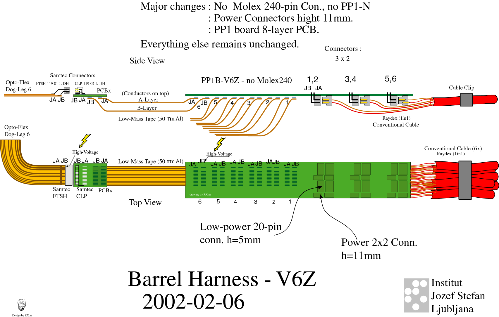
Figure1:View of PPB1, tapes and cables
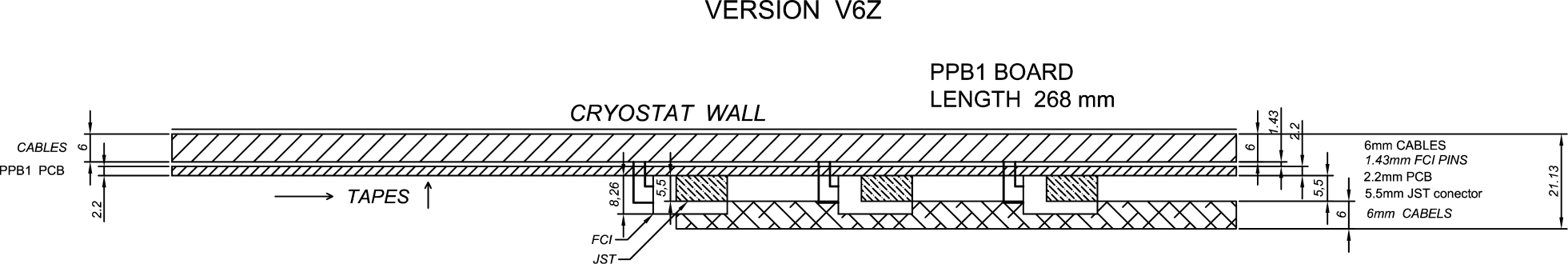
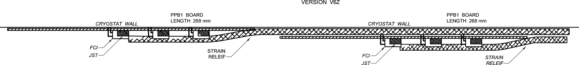
Figure 2: One and two PPB1 mounted on the cryostat wall
3. PPB1
3.1 DESCRIPTION
PPB1 accommodates the aluminum low mass tapes on the module side and conventional cables with connectors on the power supply side. One conventional cable accomodates two connectors (4 pin JST for power lines and 20 pin FCI connector for other lines). The design of PPB1 PCB has following features:
it provides soldering pads for thermode soldering of the low mass tapes to the printed circuit. Pad pattern was designed after thermode soldering tests done at Rutherford
it accepts six double layer aluminum low mass tapes, which means that it serves six modules in one harness
it provides filtering of the noise on the electrical lines
the conventional cable shield foil will be in electrical contact with a digital ground layer of the PPB1. The electrical contact is made with a conductive cable clip
it is designed in eight layers, with three layers having a large surface with a shield
mounting screws are connected to the shield plane
copper conductor thickness is 35 microns
the design obeys 2.5 mm distance (required by IPC-2221 Generic Standard on Printed Board Design) between the HV and other lines on the PCB surface
several pins will be removed from FCI connectors to conform with the HV rule
3.2 PHYSICAL DIMENSIONS
width 38 0.2 mm
length 268 0.3mm
PCB thickness 2.2 0.2 mm
3.3 ELECTRICAL LAYOUT OF PPB1
The electrical design of the board is based on the studies made in the system test and is called PPB1-V6Z. The schematic is shown in Figure 3. It provides filtering of HF noise. PPB1-V6Z is an evolution of PP1N-V3 and PP1W-V3 assembly used in the system test with the following changes:
- integration of two boards into one board with 8 layers
- connectors (4 pin FCI and 20 pin JST) will be used to connect type
II cables (Raydex AWG 20).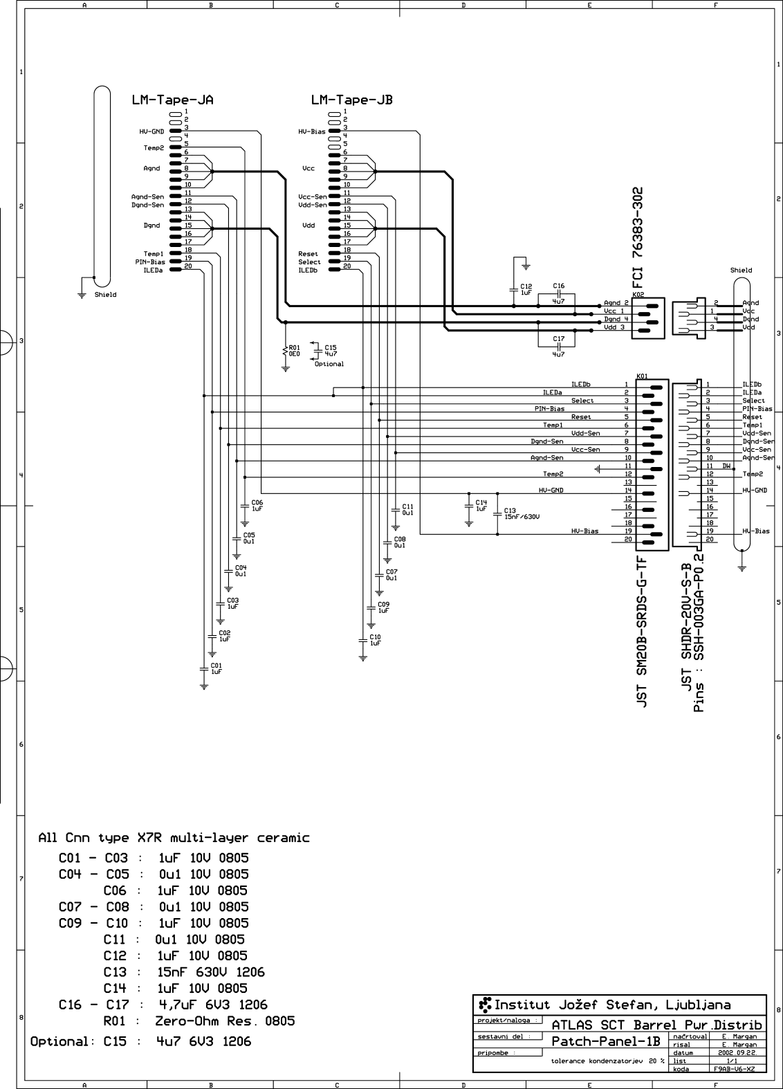
Figure 3: Schematic for PPB1
Filtering of noise is provided with capacitors. Main features are:
4.7F capacitors from Vcc, Vdd to their return lines (Murata GRM31CR61A475KA01K – size 1206, 10V)
15 nF from HV to its return line (Murata GRM31CR72J153KW03L – size 1206, 630V)
0.1F from sense, their returns, reset lines to the shield layer (Murata GRM21BR71E104KA01K – size 0805, 25V)
1 F from Temp1, Temp2, Vcsela, Vcselb, Select, Pin bias, HVgnd and Agnd
to the shield plane (Murata Murata GRM21BR71C105KA01K – size 0805, 16V)
- zero ohm resistor or optional 1F between Dgnd and shield
3.4 Pads for low mass tape soldering AND PIN
DEFINITION On FCI and JST CONNECTOR
The pads for the layout of the thermode soldering of the LMTs to PPB1 are shown Figure 4 in below.
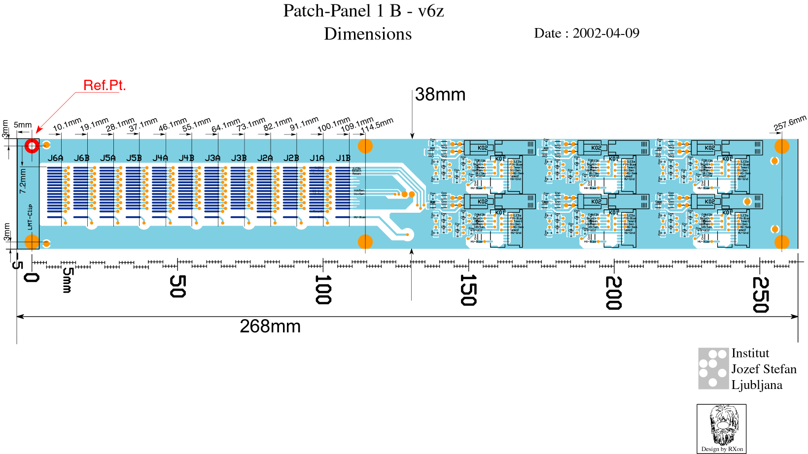
Figure 4 Layout of pads on PP1B

Figure 5: Pin definition on FCI and JST connectors
3References
1 Low Mass Tapes, EDMS ATLS-IS-AT-0010
2 MT Connectors, Spring Clips and Infineon Connectors, EDMS ATL-IS-ES-0053.
Tags: atlises0057, fibres
- OKRUHY OTÁZEK KE STÁTNÍ ZKOUŠCE (SOUBORNÉ ZKOUŠCE) Z VEDLEJŠÍ
- RADICACIÓN N˚ 95621 TUTELA 2ª INSTANCIA JUAN VIDALES DAVID
- I’M SORRY I’M SORRY TO SEE YOU’RE IN MY
- !DOCTYPE HTMLHTML LANGENHEADMETA CHARSETUTF8LINK RELICON HREFFAVICONICOMETA NAMEVIEWPORT CONTENTWIDTHDEVICEWIDTHINITIALSCALE1META NAMETHEMECOLOR
- FCC SİRKÜLER RAPOR 02244435538 02244435539 ÜÇEVLER
- CONFIDENTIALITY (WITHIN THE DOCUMENT ANY REFERENCE TO GOVERNING BODY
- FUNCANORTE FUNDACIÓN CANARIA PARA LA PROMOCIÓN DE LA CULTURA
- IMPLEMENTING ELECTRICITY RESTRUCTURING POLICIES POTHOLES AND PROSPECTS TIMOTHY J
- POLICE OFFICER POSTING POLICY THE STRUCTURE WITHIN HAMPSHIRE CONSTABULARY
- LUNEDI’ 19 MARZO FUNCTIONS SKILLS GRAMMAR LEXIS
- LINE 1 NAVODILA O UPRAVIČENIH STROŠKIH ZA SREDSTVA EVROPSKE
- F ER FRANS SA L’AGÈNCIA DE VIATGES RBLA SANT
- ELEKTRONİK CİHAZ SİGORTASI GENEL ŞARTLARI TEMINAT KAPSAMI MADDE 1
- OFT 1 OFT 1 ORDENANÇA FISCAL REGULADORA DE LA
- TAŞINIR İSTEK BELGESİ İSTEK YAPAN BIRIM BESYO TARIH
- PROF MONHEIM VORLESUNG VERKEHR LITERATURÜBERSICHT LEHRBÜCHER FETT UND KURSIV
- OPERADORES EN ESPACIOS CON PRODUCTO INTERNO DEFINICIÓN SEA UN
- EL MODELO OFRECE ALTAS PRESTACIONES TECNOLÓGICAS SIN DEJAR DE
- 0 COMUNIDAD ANDINA SECRETARIA GENERAL RESOLUCIÓN 054
- STRATEGIJA RAZVOJA OPĆINE DARDA 2016 – 2021 SADRŽAJ 1
- [COUNCIL NAME] WHISTLEBLOWER TRACKING REPORT DATE SUBMITTED TRACKING NUMBER
- GENTOFTE KOMMUNE DAGSORDEN TIL MØDE I BØRNE OG SKOLEUDVALGET
- Schools Workforce Development Strategy Contents 1 Executive Summary 2
- THE NURSING WORKFORCE AND WORKPLACE EMOTION WORK IN CLINICAL
- DECONSTRUCTING RACE CLASS AND GENDER INEQUALITY IN PERSONAL EARNINGS
- NUMER OGŁOSZENIA 113891 2010 DATA ZAMIESZCZENIA 07052010 OGŁOSZENIE
- DESARROLLO DE ALGUNOS ASPECTOS DE LA LEY ORGANICA DEL
- THE PERIOD OF FINANCIAL DISTRESS IN SPECULATIVE MARKETS INTERACTING
- ESTATUTO DE LA VÍCTIMA DEL DELITO TRASCENDENCIA DE UNA
- HALVÅRSPLAN I MATEMATIKK 7 TRINN HAUSTEN 2017 VEKE LÆREPLANMÅL
 INTEGRATION OF CREDIT MARKET AND OPERATIONAL RISK A COMPARATIVE
 TRIGONOMETRÍA ANGULO Y SUS MEDIDAS EN ADELANTE CONCEBIREMOS
PROCEDURA WYBORU CZŁONKÓW RADY RODZICÓW PRZY SZKOLE PODSTAWOWEJ NR
 GROUP 5 LAMPIRAN SURAT EDARAN BERSAMA MENTERI KEUANGAN DAN
TITLE I ANNUAL PARENT MEETING [DATE] [TIME] [LOCATION] PLEASE
PO VII WB 261142018 KIELCE 11 LIPCA 2018 R
COLORADO EXHIBIT F – CMS 43610 DEALER AGREEMENT
 CONTOH FORMAT PERMOHONAN PENCAIRAN BANTUAN KEUANGAN BHBK FISIK
PISMO 4 STUDENOG 2015 POVODOM GODINE MILOSRĐA SADRŽAJ
 TALLERES REGIONALES DIRIGIDOS A LOS GRUPOS ÉTNICOS “LA
 EL PASADO 11 DE JULIO ADRIAN SUFRIÓ UN
DİAFONOSKOP CİHAZI TEKNİK ŞARTNAMESİ 1 PREMATÜRE VE NEONATAL HASTALARIN
 …………………………………… PIECZĘĆ GMINY FORMULARZ „ZESTAWIENIE STRAT PONIESIONYCH PRZEZ JEDNOSTKI
AGREEMENT FOR USE OF CHURCH HALL OR CHURCH PARTIAL
 PAUTA ACTIVIDAD CHILE Y SU PRODUCCIÓN DE RECURSOS OBSERVE
 JURISDICCIÓNCONTENCIOSOADMINISTRATIVA RECURSO DE APELACIÓN NÚM 362003 PONENTE ILMO SR
 FICHA TÉCNICA 1 DENOMINACIÓN DEL MEDICAMENTO VETERINARIO SYVAQUINOL 25
NUMBER AS91179 VERSION 2 PAGE 2 OF 2 ACHIEVEMENT
VICTORIA LEGAL AID SEX OFFENDER PROHIBITION ORDERS – OVERVIEW
 AKTUALISIEREN DER FIRMWARE DES ALARMMELDER MOBILFUNK WICHTIG VERFAHREN SIE
