BOND TESTS ON PRINTED CIRCUIT BOARDS WITH PALLADIUM METALLIZATIONS
01 SEP 09 | UTILIDAD DE LOS TESTS DIAGNÓSTICO1 CALIBRATION AND RELIABILITY TESTS OF ENVIRONMENTAL MOBILE SENSORS
1 TESTS OF BETWEENSUBJECTS EFFECTS DEPENDENT VARIABLEPAPER SOURCE TYPE
1 TESTS OF BETWEENSUBJECTS EFFECTS DEPENDENT VARIABLETOWNTRIPS SOURCE TYPE
1 UZDEVUMS – TESTS 1 ATVER DOKUMENTU TESTS2014DOCX NO
15A NCAC 02B 0508 TESTS AND MEASUREMENTS APPLICABLE TO
Bond tests on Printed Circuit Boards with Palladium Metallizations
Bond tests on Printed Circuit Boards with Palladium Metallizations
Ian Mcgill and Christian Joram – PH/TA1/SD
May 2004
Bond tests were performed on two PCB samples fabricated by the French company CIRLY1. The samples feature Copper (Cu) soldering pads, which are electrolytically coated with a 0.2 m thick layer of Palladium (Pd). Some information on the advantages of Palladium is given in the annex at the end of this document.
Bond equipment:
Delvotec 6400 aluminium wedge bonder(45deg feed angle), tool 4W4F-1820-W7C_F00, wire 25micron Al/1%Si, US frequency 100 kHz
Testing equipment:
Wire pull tester, Dage type 2400A, geometry 30degree pull on 1st and 2nd bonds. The bondwire length was 1.5mm.
Performed tests:
3 sets of bond tests with 10 wires each were made changing the following parameters
|
Parameter |
Set.1 |
Set.2 |
Set.3 |
|
Ultrasonic Power2 |
75 |
70 |
75 |
|
Bond Force |
125 |
100 |
100 |
|
Touch Down Force |
115 |
90 |
90 |
|
US Power Max. |
20 |
20 |
20 |
|
US Power Min |
75 |
70 |
75 |
The following relevant parameters were kept constant for all sets.
|
Parameter |
value |
|
Deformation |
70 |
|
Rampsteps |
250 |
|
Bond delay |
20ms |
|
Touch down delay |
10ms |
|
Curvescale |
1150 |
|
TD Delay |
10ms |
|
Td Offset |
20 |
|
TD Steps |
2 |
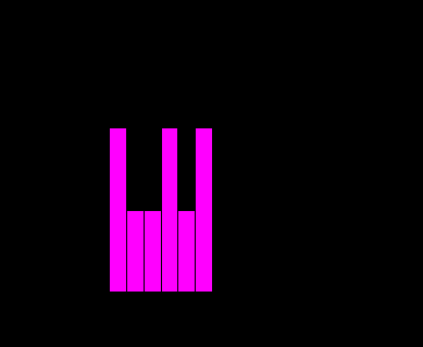
The statistical analysis gave the following results.
|
Set.1 Set.2 Set.3 |
|
Min: 10.41 10.45 10.13 |
|
Mean: 10.70 10.86 10.498 |
|
Max: 10.97 11.21 10.73 |
|
Std Dev.: 0.206 0.252 0.254 |
The 3 parameter sets give good pull tests results. The failure mode is in practically all cases ‘First heel failure’ as it should be. Set 1 is believed to give the best results in terms of surface variability.
Some tests were carried out using a lower deformation of 65. This also gave good results, but to allow for surface variability and flaws the slightly higher deformation should be more consistent.

Further tests
2 sets of bond tests with 10 wires each were made changing the following parameters
|
parameter |
Set.4 |
Set.5 |
|
Ultrasonic Power3 |
75 |
75 |
|
Bond Force |
140 |
125 |
|
Touch Down Force |
130 |
115 |
|
Us Power Max |
20 |
15 |
|
Us Power Min |
75 |
75 |
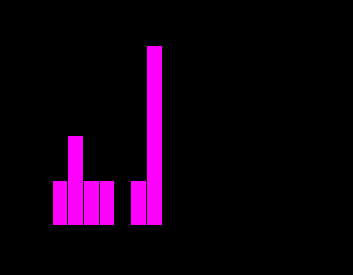
Set.4 failure modes: 6 x Second Bond Lift, 1 x Midwire Break, 3 x First Heel Failure
Set.5 failure modes: 2 x Second Bond Lift, 2 x Midwire Break, 5 x First Heel Failure
The statistical analysis gave the following results:
|
Set.4 Set.5 |
|
Min: 7.61 10.33 |
|
Mean: 9.37 10.87 |
|
Max: 10.85 11.37 |
|
Std Dev.: 1.28 0.318 |

Conclusion
Palladium coated Copper pads can be used for Aluminum wedge bonding, leading to good pull test results.
Characterization of long term reliability and behavior under special environmental conditions, e.g. high or low temperature or strong temperature variations, would require further more extensive tests.
Annex : Palladium
|
PRINCIPLE: Electrolytic plating of Palladium ( Pd) on copper. Thickness of the plating env. 0,2µm. ADVANTAGES: QUALITY Finish particularly adapted to circuits classifies 5 Good flat deposit specially useful for the soldering of SMD Good wetability, good soldering, beautiful aspect Mastery of a process which is perfectly integrated into our workshop Abolition of the lead (protection of the environment) The palladium plating is practised within weak temperatures: abolition of the thermic shocks related to the HAL Compatibility with the various types of soldering pastes excellent definition of etching Very good behaviour within the etching Does not oxidize below 400degC
Saving of time Mastery of the process internally Reliability of the delay still increased INCONVENIENCES: Palladium is a noble metal Its rate is fluctuating CHARACTERISTICS: TECHNOLOGICAL Flat plating and soudable very fine plating < or = to 0,2µm directly on the copper Allows SMD with the finest pitches which one can find today Allows the Chip On Board gold and aluminium wire systems to be used Process already used in the finish of the components. PHYSICS Hardness = 240-260 Knoop Density = 11,5-12,0 g / cm3 Internal tension= 62-64 KPSI Strain = > 6 % Structure = Equiaxiale with fine grain Dissolution of the Pd at 250°C during 3 seconds Copyright© CIRLY S.A. 2001 - Design by FORNEXT |
1 CIRCLY SA, Lyon, France. www.cirly.com
2 All numbers are machine specific and will be different on other bonding machines
3 All numbers are machine specific and will be different on other bonding machines
18 THE MISUSE OF UNIDIMENSIONAL TESTS AS A DIAGNOSTIC
211112 ACCEPTANCE TESTS BEFORE AN AERIAL TRAMWAY THAT IS
219319DOC STAND 24112008 CEZERTIFIZIERTE BZW INHOUSEVALIDIERTE SUCH UND BESTÄTIGUNGSTESTS
Tags: boards with, metallizations, boards, circuit, palladium, printed, tests
- PROTOCOLO DE SONDAJE VESICAL 1 INDICACIONES EVACUACIÓN DE
- POSKYTNUTÍ LICENCE PROHLAŠUJI TÍMTO ŽE JSEM VÝROBCEM FOTOGRAFIE
- ANALYSIS OF RAINFALL VARIABILITY IN THE KRISHNA RIVER BASIN
- FORMATO PARA LA PRESENTACIÓN DE PLAN DE MANEJO DE
- 7 MENTERI DALAM NEGERI REPUBLIK INDONESIA
- MASSIMILIANO CAPPUCCIO MIRROR NEURONS AND SKILFUL COPING MOTOR INTENTIONALITY
- RELACIONES INTERNAS POR PRESTACIÓN DE SERVICIOS RESPONSABLE DE LA
- HEALTH INFORUM NEWS ملتقى الصحة VOLUME 1 NO15 15
- GUIA LABORAL PARA LA ACCIÓN SINDICAL COMISIÓN EJECUTIVA
- CEFA L’INTERVENTION DES SECTEURS DANS L’INSERTION SOCIOPROFESSIONNELLE DES ÉLÈVES
- LE CONSEIL CONSTITUTIONNEL LE CONSEIL CONSTITUTIONNEL EST INSTITUÉ PAR
- TCIIA EVENT PAYMENT AND CANCELLATION REFUND POLICY PAYMENT FOR
- OFERTA DE EMPLEO PRIVADO EN MALAGA Y PROVINCIA ESTA
- 1 UNIWERSYTET MEDYCZNY IM PIASTÓW ŚLĄSKICH WE WROCŁAWIU KATEDRA
- NA OSNOVU ČLANA 105 ZAKONA O JAVNIM NABAVKAMA (“SLUŽBENI
- EXPTE NRO32316 R L A S CURATELA MAR DEL
- CONSENT FORM REFERENCE EXAMPLE RE ENTRY TO THE INJURY
- CHAPTERS 192 AND 193 ADDITIONAL FUNDING – 200910 FREQUENTLY
- STAR WARS HERO’S JOURNEY PROF JENN STAR WARS EPISODE
- BASIC SOIL SURVEY FIELD AND LAB (000012) OVERVIEW THIS
- PODRUČJA NATURA 2000 – OPĆINA KARLOVAC (3092011) SPA PODRUČJE
- KOPRIVNIČKOKRIŽEVAČKA ŽUPANIJA POZIV ZA PREDLAGANJE PROGRAMAPROJEKATA UDRUGA ZA DJELATNOST
- HIDROQUINONA RETINÓICO E INDOMETACINA INFORMACIÓN AL PACIENTE COMPOSICIÓN CUALITATIVA
- DECLARACIÓN RESPONSABLE DE ACREDITACIÓN DE QUE TANTO LA ENTIDAD
- NUMERO 253 EL CONGRESO DEL ESTADO LIBRE Y SOBERANO
- ACTIVIDADES FIGURAS LITERARIAS Y MÉTRICAS LENGUA CASTELLANA Y LITERATURA
- OFERTA DO POSTĘPOWANIA ZNAK ZZP21217
- BIOHUSET WWWBIOHUSETLEMVIGDK BREDGADE 17 –
- GRAD SUBOTICA MESNA ZAJEDNICA „ŽELJEZNIČKO NASELJE” SKUPŠTINA MESNE ZAJEDNICE
- STRONA 7 Z 7 SZKOLNY ZESTAW PROGRAMÓW SZKOŁY PODSTAWOWEJ
 11 PEREMPUAN PEMBUAT BATU BATA DI DESA KALE MANDALLE
WÓJT GMINY STRZELECZKI OGŁASZA NABÓR NA STANOWISKO ANIMATOR
 REQUISITOS E CONDICIONS PARA A OBTENCION DAS CARTILLAS NAUTICAS
BIO INFORMATION HUGH HOPPER TITLE HOPPER TUNITY BOX (CUNEIFORM
 PERSONAL PROTECT POLICY – INDIVIDUAL ACCIDENT INSURANCE PREAMBLE ICICI
SEMINARIO MUJER Y MIGRACIÓN EN LA REGIÓN DE LA
 INFORMASJON TIL TILTAKSHAVER OG SØKER DESEMBER 2017 BRUKSENDRING SØKNAD
VIDEO – FORMULARZE 3 PROCEDURY I DODANIE NOWEGO KLIENTA
 CURRÍCULUM NORMALITZAT NUM REGISTRE COGNOMS NOM SEXE DNI DATA
ID TO STUDENTS AND FACULTY CREATING A PRETESTING
 VISTATEC MASCARILLAS MASCARILLAS FABRICADAS CON PLÁSTICO TRANSPARENTE DE PRIMERA
ANNEX – COVER SHEET FOR RESPONSES CALL FOR EVIDENCE
 DOKUMENTATION LSMW UPLOAD AUS EXCEL EXCEL TABELLE IM
 () MODELO DE CERTIFICADO PARA LEGALIZACIÓN DE LOS LIBROS
PREDLOG ZAKONA O ZAPOŠLJAVANJU STRANACA I OSNOVNE ODREDBE PREDMET
 COMMUNITY CONVERSATIONS PHASE TWO COMMUNITY ENGAGEMENT MELTON CITY COMMUNITY
 KUATIA MOÑE’ÊRÂ GUARANÍME 2 HAI ÑEMOÑE’Ê HA MBOSA’Y HAGUÂ
HI EVERYONE THIS IS THE EIGHTH OF THE WEEKLY
 BIAŁYSTOK 14082019R ZAPYTANIE OFERTOWE NR 11CIS2019 – ROZEZNANIE CENY
A FORMULARZ 23 DO ZARZĄDZENIA NR 1807 REKTORA AWF
