BIAS SETTINGS THE BIASING OF THE ASIC IS
DATOSREADTABLE(CDOCUMENTS AND SETTINGSLETICIAMIS DOCUMENTOSESPEMULTIVARIADOSEMESTRE20131DATOSTRESPOPULATIONACTION2012TXT HEADER TRUESEP)LIBRARY(MASS) LIBRARY(CLUSTER) ARANAREADTABLE(CDOCUMENTS AND SETTINGSLETICIAMIS DOCUMENTOSESPEMULTIVARIADOSEMESTRE20091MDSARANATXT)
PALLIATIVE MEDICINE SURVEY FORM TO ACCREDIT TRAINING SETTINGS
!doctype Htmlhtml Langhr Class Sidebarsettings head meta Charsetutf8
0 PREDICTING COMPARISON CHOICES IN INTERGROUP SETTINGS A NEW
10 MARANTZ AUDIO RECORDER SETTINGS RUNCOCO UNIVERSITY OF OXFORD
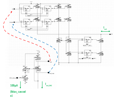
Bias settings:
The biasing of the ASIC is designed to allow a great degree of versatility: this is achieved by a number of on-chip Digital-to-Analogue Converters (DACs), either 4 or 8 bit resolution, which set many of the bias voltages used in the chip.
All the DACs are implemented with a binary-weighted current-switched architecture: the control bits set the ratio for mirroring a reference current into a resistor, which converts this current into voltage.
The DACs differs in:
Resolution: 4 or 8 bit
Polarity: pMOS are used as current mirrors when the desired output is in the upper voltage range (up to vdd); nMOS when the ouput is closer to gnd (fig.1)
Range: the values of the reference current and of the integrated resistor are designed to match the desired output range
Offset: some of the bias voltages are offset, in order to centre the output range on the most suitable value. For these voltages is not possible to reach vdd or gnd, as a non-zero current is always sunk or sourced into the resistor.
Cascode architecture: the most sensitive bias references (e.g. the comparators’ threshold) are generated by wide-swing cascode current mirrors, which allow enhanced performances without limiting the signal swing available (fig2)
Output buffer: to provide drive strength or to minimize crosstalk, some of the DACs’ output voltages are buffered (either locally or within each channel)
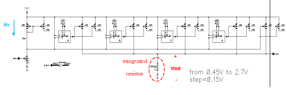
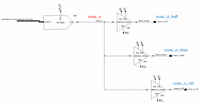
Fig 1a: 4bits pmos-type DAC; output voltage across the resistor to gnd
F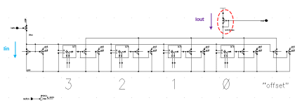
ig
1b: 4bit nmos-type DAC; output current to be mirrored to the
following stage. In this case besides the 4 bit-controlled branches,
there is an additional one to generate an output offset
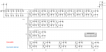


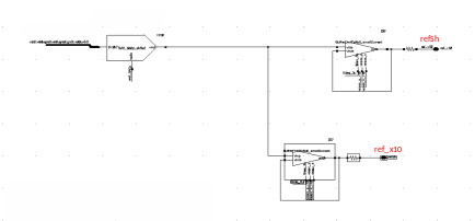
Fig2: 8bit nmos-type DAC with cascode architecture
DAC description table:
|
|
control bits |
output |
bits |
Type |
Iref, mirror factor, R* |
Offset |
Range |
Cascode |
|
1 |
<45:48> |
clamp_thresh |
4 |
p |
Iref=25μA Iout=[0:15/16Iref] R*=96kΩ |
3/16 Iref |
Vout=[0.45÷2.7V] |
no |
|
2 |
<49:56> |
vin_compThresh vin_casc_CompThresh |
8 |
n |
Iref=25μA Iout=[0:255/64Iref] |
0 |
Iout=[0÷99.6μA] |
yes |
|
3 |
<57:64> |
ref_x10/refSh |
8 |
p |
Iref=60μA Iout=[0:255/16Iref] R*=2400Ω |
53/16Iref |
Vout=[477mV÷2.77V] |
no |
|
4 |
<65:72> |
vin_fastCompThresh_HEC vin_casc_fastCompThresh_HEC |
8 |
n |
Iref=25μA Iout=[0:255/64Iref] |
0 |
Iout=[0÷99.6μA] |
yes |
|
5 |
<73:80> |
vin_fastCompThresh vin_casc_fastCompThresh |
8 |
n |
Iref=25μA Iout=[0:255/64Iref] |
0 |
Iout=[0÷99.6μA] |
yes |
|
6 |
<81:88> |
vcasc_n |
8 |
n |
Iref=60 μA Iout=[0:255/16Iref] R*=2560Ω |
0 |
Vout=[0÷2.45V] ** |
no |
|
7 |
<89:96> |
vcasc_p |
8 |
n |
Iref=60 μA Iout=[0:255/16Iref] R*=2560Ω |
0 |
Vout=[0÷2.45V] ** |
no |
|
8 |
<97:104> |
ref |
8 |
p |
Iref=60μA Iout=[0:255/16Iref] R*=2400Ω |
0 |
Vout=[0÷2.45V]*** |
no |
|
9 |
<105:112> |
biasRC_preAmp_HEC |
8 |
p |
Iref=60μA Iout=[0:255/16Iref] R*=2400Ω |
0 |
Vout=[0÷2.295V]** |
no |
|
10 |
<113:120> |
vcasc_preAmp_HEC |
8 |
p |
Iref=60μA Iout=[0:255/16Iref] R*=2400Ω |
0 |
Vout=[0÷2.295V]** |
no |
|
11 |
<121:124> |
Ibias_LFfdbk |
4 |
n |
Iref=160uA Iout=[0:15/16Iref] |
1/16 Iref |
Iout=[10μA÷160μA] |
no |
|
12 |
<125:132> |
biasRC_preAmp |
8 |
p |
Iref=60μA Iout=[0:255/16Iref] R*=2400Ω |
0 |
Vout=[0÷2.295V]** |
no |
|
13 |
<133:136> |
Ibias_preAmp_SF |
4 |
n |
Iref=25 μA Iout=[0:15/16Iref] |
8/16 Iref |
Iout=[2.5mA÷7.5mA] |
no |
|
14 |
<137:144> |
vcasc_preAmp |
8 |
p |
Iref=60μA Iout=[0:255/16Iref] R*=2400Ω |
0 |
Vout=[0÷2.295V]** |
no |
|
15 |
<145:148> |
Ibias_preAmp |
4 |
n |
Iref=25 μA Iout=[0:15/16Iref] |
8/16 Iref |
Iout=[556μA÷1.6mA] |
no |
|
16 |
<149:156> |
threshold_link |
8 |
|
Iref=60μA Iout=[0:255/16Iref] R*=2400Ω |
0 |
Vout=[0÷2.295V] |
no |
* nominal value; real value in the range [nominal value±30%]
**Effective output voltage limited by the following buffer stage in the range [0.5÷2.3V]
***Effective output voltage limited by the following buffer stage in the range [0.1÷3.1V]
Biasing voltages:
clamp_thresh
This is the reference voltage for the comparator which clamps the x10 gain stage to a unity gain configuration. The aim of the clamping is to avoid saturation of the amplifier in the x10 gain stage, therefore the clamp_thresh must be set just above or below the linear region of the amplifier (according to the polarity selected):
-
x10 reference
clamp_thresh
1 V (positive polarity)
>2.4 V
2.4 V (negative polarity)
<1 V
N.B.: if the x10 reference is changed then the clamp_thresh value must track it as stated above
Because a fine tuning of this value is not necessary, as long as saturation is avoided, a 4 bit DAC is adequate:
-
control bits
clamp_thresh
x [0÷15]
((x+3)/16)*25μA*96KΩ
0000
0.45V
0001
150mV
…
…
1111
2.7V
-
Default value
positive polarity: 1101
2.4V
negative polarity: 0100
1.05V
vin_compThresh / vin_casc_compThresh
T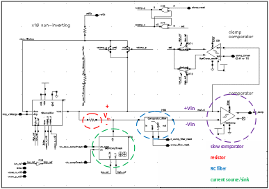
hese
two voltages set the threshold for the “slow” (low noise)
comparator which follows the x10 gain stage. Because the baseline of
this comparator is derived from the x10 gain stage’s output, it
would not be possible to set it to an absolute value without
introducing an offset error
The baseline of the comparator is derived from the x10 stage’s output, therefore to avoid introducing an offset the threshold value must be derived from the same baseline too. This is achieved by sinking or sourcing a selectable current across a resistor between the two comparator’s inputs:
The value of the resistor is R=17.5KΩ, the selectable current Iout=[0÷99.6μA]; this current is sourced or sunk into the resistor according to the selected polarity (this is controlled by the control bit…). The threshold voltage is therefore in the range |Vth|=[0÷1.750V]
-
control bits
Iout
|Vth|
x [0÷255]
(x/64)*25μA
(x/64)*25μA *17.5KΩ
00000000
0 A
0 V
00000001
0.39 μA
6.825mV
…
…
…
11111111
99.6 μA
1.750V
vin_compThresh
and vin_casc_compThresh are connected to two output PADs each (top
and bottom of the ASIC).
-
Default value
positive polarity: 00001111
0.102V
negative polarity: 00001111
0.102V
ref_x10 - refSh
The
input references of both shaper and x10 gain stage are the buffered
output of a common 8bit DAC’s output:
-
control bits
refSh – ref_x10
x [0÷255]
((x+53)/16)*60μA*2.4KΩ
00000000
477mV
00000001
486mV
…
…
11111111
2.772V
Default value
positive polarity: 00110100
0.945 V
negative polarity: 11010011
2.376 V
ref_x10 and refSh are connected to two PADs each (top and bottom of the ASIC).
It is recommended to load these two nets with external capacitors, for improved stability and noise performance:
-
external capacitance
ESR (equivalence series resistance)
refSh
C≥1μF
ESR≤1Ω (possibly less)
ref_x10
C≥1μF
ESR≤1Ω
vin_fastCompThresh_HEC – vin_casc_fastCompThresh_HEC
T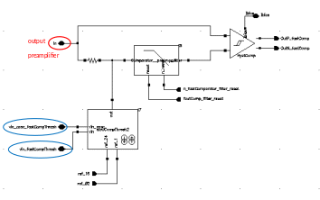
hese
two voltages set the threshold for the fast (high noise) comparator
that follows the HEC preamplifier. The technique is the same as the
one described in point2.
Again, the value of the resistor is R=17.5KΩ, the selectable current Iout=[0÷99.6μA]; this current is sourced or sunk into the resistor according to the selected polarity (this is controlled by the control bit…). The threshold voltage is therefore in the range |Vth|=[0÷1.750V]
-
control bits
Iout
|Vth|
x [0÷255]
(x/64)*25μA
(x/64)*25μA *17.5KΩ
00000000
0 A
0 V
00000001
0.39 μA
6.825mV
…
…
…
11111111
99.6 μA
1.750V
-
Default value
positive polarity: 00001111
102.5V
negative polarity: 00001111
102.5V
vin_fastCompThresh – vin_casc_fastCompThresh
As in point4, for Low Energy Channel.
vin_fastCompThresh and vin_casc_fastCompThresh are connected to two PADs each (top and bottom of the ASIC).
-
Default value
positive polarity: 00001111
102.5V
negative polarity: 00001111
102.5V
vcasc_n ( vcasc_n_buff, vcasc_n_shap, vcasc_n_x10)
The output of an 8bit n-type DAC is buffered to generate the cascode voltage (nmos) for shaper’s, high speed buffer’s and x10 gain stage’s amplifiers:
-
control bits
vcasc_n
x [0÷255]
Vdd - [(x/16)*60μA*2.56KΩ]
00000000
Vdd
00000001
Vdd – 9.6mV
…
…
11111111
Vdd – 2.448V
-
Default value
positive polarity: 11010010
1.284V
negative polarity: 11010010
1.284V
vcasc_p ( vcasc_p_buff, vcasc_p_shap, vcasc_p_x10)
The same as vcasc_n (point6), but in this case the cascode is a pmos-type (so vcasc_p is set to a higher value than vcasc_n).
-
Default value
positive polarity: 10000000
2.071V
negative polarity: 10000000
2.071V
ref
ref is a global reference which is buffered locally (inside each channel) to generate the reference input voltages for the LEC’s and the HEC’s preamplifiers.
-
control bits
ref
x [0÷255]
(x/16)*60μA*2.4KΩ
00000000
0 V
00000001
9 mV
…
…
11111111
2.295 V
-
Default value
positive polarity: 10110010
1.602V
negative polarity: 00010110
0.198V
ref is connected to two PADs (top and bottom of the ASIC).
biasRC_preAmp_HEC
This is the gate voltage of the active transistor active as a resistor in the preamplifier’s compensation circuit. An adjustment of this value may be necessary to ensure stability when operating with different values for the detector capacitance.
-
control bits
biasRC_preAmp_HEC
x [0÷255]
(x/16)*60μA*2.4KΩ
00000000
0 V
00000001
9 mV
…
…
11111111
2.295 V
-
Default value
positive polarity: 01011100
0.828V
negative polarity: 01011100
0.828V
This voltage is buffered globally, and connected to two output PADs (top and bottom of the ASIC).
vcasc_preAmp_HEC
cascode voltage (nmos cascode) for the HEC preamplifier. This voltage is buffered globally.
-
control bits
vcasc_preAmp_HEC
x [0÷255]
(x/16)*60μA*2.4KΩ
00000000
0 V
00000001
9 mV
…
…
11111111
2.295 V
-
Default value
positive polarity: 01101000
0.936V
negative polarity: 01101000
0.936V
Ibias_LFfdbk
Ibias_LFfdbk sets the bias current for the Low Frequency Feedback (LFfdbk) of the preamplifier. It is mirrored locally in each LFfdbk block and scaled down to 1/104 of the original value.
-
control bits
Ibias_LFfdbk
x [0÷15]
((x+1)/16)*160μA
0000
10 μA
0001
20 μA
…
…
1111
160 μA
-
Default value
positive polarity: 0000
10 μA
negative polarity: 0000
10 μA
biasRC_preAmp
like biasRC_preAmp_HEC (point 9), for LEC. This voltage is buffered globally.
biasRC_preAmp is connected to two output PADs (top and bottom of the ASIC).
-
Default value
positive polarity: 01011100
0.828V
negative polarity: 01011100
0.828V
Ibias_preAmp_SF
bias current for the output stage of the preamplifier (Source Follower), for both LEC and HEC.
-
control bits
Ibias_preAmp_SF
I_SF (Source Follower’s current)
x [0÷15]
((x+8)/16)*25μA
200*((x+8)/16)*25μA
0000
12.5 μA
2.5 mA
0001
14.06 μA
2.81 mA
…
…
…
1111
35.94 μA
7.5 mA
-
Default value
I_SF
positive polarity: 1000
5mA
negative polarity: 1000
5mA
vcasc_preAmp
like vcasc_preAmp_HEC (point10), for LEC. This voltage is buffered globally.
vcasc_preAmp_HEC is connected to two output PADs (top and bottom of the ASIC).
Simulations have shown a crosstalk reduction when this net is loaded with an external capacitor C≥100nF.
-
Default value
positive polarity: 01101000
0.936V
negative polarity: 01101000
0.936V
Ibias_preAmp
bias current for the preamp (first two stages, not Source Follower).
-
control bits
Ibias_preAmp
Itail first stage
Ibias second stage
x [0÷15]
((x+8)/16)*25μA
84*((x+8)/16)*25μA
44.5*((x+8)/16)*25 μA
0000
12.5 μA
1.05 mA
556 μA
0001
14.06 μA
1.181 mA
626 μA
…
…
…
…
1111
35.94 μA
3.019 mA
1.6 mA
-
Default value
positive polarity: 1000
1.112 mA
negative polarity: 1000
1.112 mA
threshold_link
This is the reference voltage for the comparator which controls the clamp switch across the link diodes. It must be set to a value above or below the preamplifier’s input reference voltage, according to the chosen polarity:
-
input reference
threshold_link
0.2V (negative polarity)
<0.2V
1.6V (positive polarity)
>1.6V
N.B.: if the input reference is changed then the threshold_link value must track it as stated above
-
control bits
threshold_link
x [0÷255]
(x/16)*60μA*2.4KΩ
00000000
0V
00000001
9mV
…
…
11111111
2.295V
-
Default value
positive polarity: 10101010
1.530V
negative polarity: 00010100
0.180 V
threshold_link is connected to two output PADs (top and bottom of the ASIC).
11 MULTICULTURAL COUNSELING IN EDUCATIONAL SETTINGS CLED 607 REF
3 ELEMENTARY LESSON PLAN (STRUCTURAL APPROACH) RECOGNIZING COMMUNITY SETTINGS
7 THE EARLY HELP SERVICES AND UNIVERSAL SETTINGS THE
Tags: biasing of, [0.1÷3.1v] biasing, biasing, settings
- DEPARTMENT OF THE INTERIOR DEPARTMENTAL MANUAL EFFECTIVE DATE 91889
- INSTRUKCJA ZWROTU OPŁAT REKRUTACYJNYCH ZWROT OPŁAT REKRUTACYJNYCH 1 WNIOSKOWAĆ
- FAMILY ACCESS NETWORK FAMILY ACCESS NETWORK IS COMMITTED TO
- USNESENÍ Č 752900 PŘÍLOHA Č 1 STRANA 4
- TEACHERS VIBEKE JULIE PHIL SCIENTISTS ANTONIO JUTTA ANNETTE MAX
- PRIOPĆENJE ZA JAVNOST 5 JUBILARNI SAJAM STIPENDIJA NA OVOGODIŠNJEM
- FS AGENCY REGULATIONS AND POLICY FOREST PLANNING REGULATIONS 36
- EXCMO AYUNTAMIENTO DE SALAMANCA ÁREA DE BIENESTAR SOCIAL SECCIÓN
- 2 РОССИЙСКАЯ ФЕДЕРАЦИЯ ИЗБИРАТЕЛЬНАЯ КОМИССИЯ ИРКУТСКОЙ ОБЛАСТИ П О
- DRSC NEVEN ŠERIĆ DIPLOECC CREATING OF MARKET FACTORS IN
- 23 A CLASSIC SEMINARY EDUCATION MY RECOMMENDED READING LIST
- REDISTRIBUIÇÃO DEFINIÇÃO DO SERVIÇO É O DESLOCAMENTO DE CARGO
- 様式第十六(二)(第三十三条、第百三十七条の十六関係) FORM NO 16 (2) (RELATED TO ARTICLE 33
- EJERCICIOS OPCIONALES DEL TEMA 2 CAMPO GRAVITATORIO PG 67
- 19 DOPRAVA INFORMAČNÍ A KOMUNIKAČNÍ ČINNOSTI TATO KAPITOLA OBSAHUJE
- INSTRUCTIVO ASISTENCIA TÉCNICA PROGRAMA MECESUP 2 INSTRUCTIVO PARA LA
- ÚTMUTATÓ A TUDOMÁNYOSOKTATÁSI TEVÉKENYSÉGET ISMERTETŐ ÉVES BESZÁMOLÓ ELKÉSZÍTÉSÉHEZ I
- SOLICITUD DE MODIFICACIÓN COMO CONSECUENCIA DEL COVID19 DE INTERVENCIONES
- BESZÁMOLÓ A SZÉKESFEHÉRVÁR VÁROSI TERMÉSZETBARÁT SZÖVETSÉG 2018 ÉVI TEVÉKENYSÉGÉRŐL
- VŠEOBECNÉ PODMÍNKY SOUTĚŽE SPOLEČNOSTI NEJ TV AS MAJITELE A
- MINUTES 2008 BUSINESS MEETING MRCSOT THE MIDWEST REGIONAL CHAPTER
- CURRICULUM VITAE DR IR ROELAND CE KINDT 2003 –
- PAPEL TIMBRADO DA EMPRESA COM RESPECTIVO CNPJ DECLARAÇÃO DE
- EVALUATION AND STRUCTURE OF COMMERCIAL BANKS IN INDIA VINOD
- ARCHDIOCESE OF INDIANAPOLIS WEDDING POLICIES A THE ARCHDIOCESE OF
- THE GETTY ADVANCED SEARCH HOME VISIT THE GETTY THE
- 6 A NECESIDADE DA PARTICIPACIÓN PLENA DOS MAIORES NA
- MEDIJSKA KULTURA – KAZALIŠTE KAZALIŠTE – KUĆA U
- B OLETO DE COMPRAVENTA DE CEREALES OLEAGINOSOS Y DEMAS
- COMMUNITY SCHOOL DEED OF TRUST AMALGAMATED SCHOOL MODEL LEASE
 HRVATSKA UDRUGA ZA ZAŠTITU POTROŠAČA WWWHUZPHR HUZPZGTCOMHR OZALJSKA 93II
AKILCI TIBBİ GÖRÜNTÜLEME KULLANIMI AĞIZ DİŞ VE ÇENE RADYOLOJİSİ
NEW 2012 CBHI FORM NO 2A MONTHLY MONTHLY REPORT
 U NIVERSIDAD NACIONAL MAYOR DE SAN MARCOS FUNDADA EN
[NEURE319] POSSIBILITY TO REUSE DEFINED ACTIONS CREATED 01SEP2014 UPDATED
SKY SUBSCRIBER SERVICES LIMITED CUSTOMER RELATIONS PO BOX 43
NA PODLAGI 10 ČLENA ZAKONA O ŠPORTU (UR LIST
ŻYJEMY W ŚWIECIE ORGANIZACJI ZARZĄDZANIE DZIAŁANIE WŁAŚCIWE CZŁOWIEKOWI OD
MIAPE MASS SPECTROMETRY PIERREALAIN BINZ[12] CHRIS F TAYLOR[3] RUEDI
 IN DEZE FOLDER KUNT U INFORMATIE LEZEN OVER DE
PROTOCOL ON THE ACCESSION OF THE PEOPLES REPUBLIC OF
 S AJÁT CSALÁDI HÁTTÉR FELTÁRÁSA KÉRDÉSEK A CSALÁDRÓL „LÉTEZIK
 MÅNADSRAPPORT – OKTOBER BUDGETEN 2012 ÄR LIKSOM FÖREGÅENDE ÅR
 INFORME DT POSTERIOR A LA COMPETICION COMPETICION LUGAR Y
 FORMATO PARA LA ATENCIÓN DE DENUNCIAS RECIBIDAS POR EL
CHAIRMAN’S REPORT TUDOR SQUARES ANNUAL GENERAL MEETING 13 OCTOBER
1 TARAFLAR İŞ BU SÖZLEŞME ULUSLARARASI SATIŞ VE PAZARLAMA
 AMONTUORI OLTRE IL ROMANTICISMO 1 SIMBOLISMO E DECADENTISMO 2
SDSU SOCIOLOGY & RURAL STUDIES GRADUATE STUDENT REQUEST FOR
 HVORDAN FORBINDER MAN SÆTNINGER PÅ JAPANSK? てFORM 本や に
